[0006]The present invention provides a novel method and apparatus for manufacturing three-dimensional, high density, integrated circuit modules from standard ball-grid-array or other surface
mount integrated circuit packages which provides improved space efficiency and heat dissipation. One way to increase space efficiency is to stack individual packages. Generally speaking, higher density generates more localized heat and thus increases the need for efficient heat dissipation. Improving the
thermal transfer characteristics of the individual integrated circuit packages results in better heat dissipation for the module, and improves reliability and durability.
[0007]The present invention provides a novel method of fabricating a three-dimensional module formed of stacked and aligned surface
mount or ball-grid-array packages. Ball-Grid-Array (BGA) integrated circuit packages typically have leads that extend from the bottom surface of a rectangular
solid resin casing in a two-dimensional
grid pattern. The external portion of each lead finished with a ball of solder.
Package leads provide electrical and
thermal coupling to one or more integrated circuit dies that are embedded within the protective casing. Typically, the protective casing completely surrounds the embedded die but, in some BGA packages, the protective casing does not cover the inactive top surface of the die. Near-
chip scale packages provide 1.0 mm center-to-center lead spacing.
Chip scale packaging such as MICRO_BGA™ have center-to-center lead spacing of 0.5 mm.
Chip scale packaging offers excellent electrical characteristics including low
capacitance and thermal design.
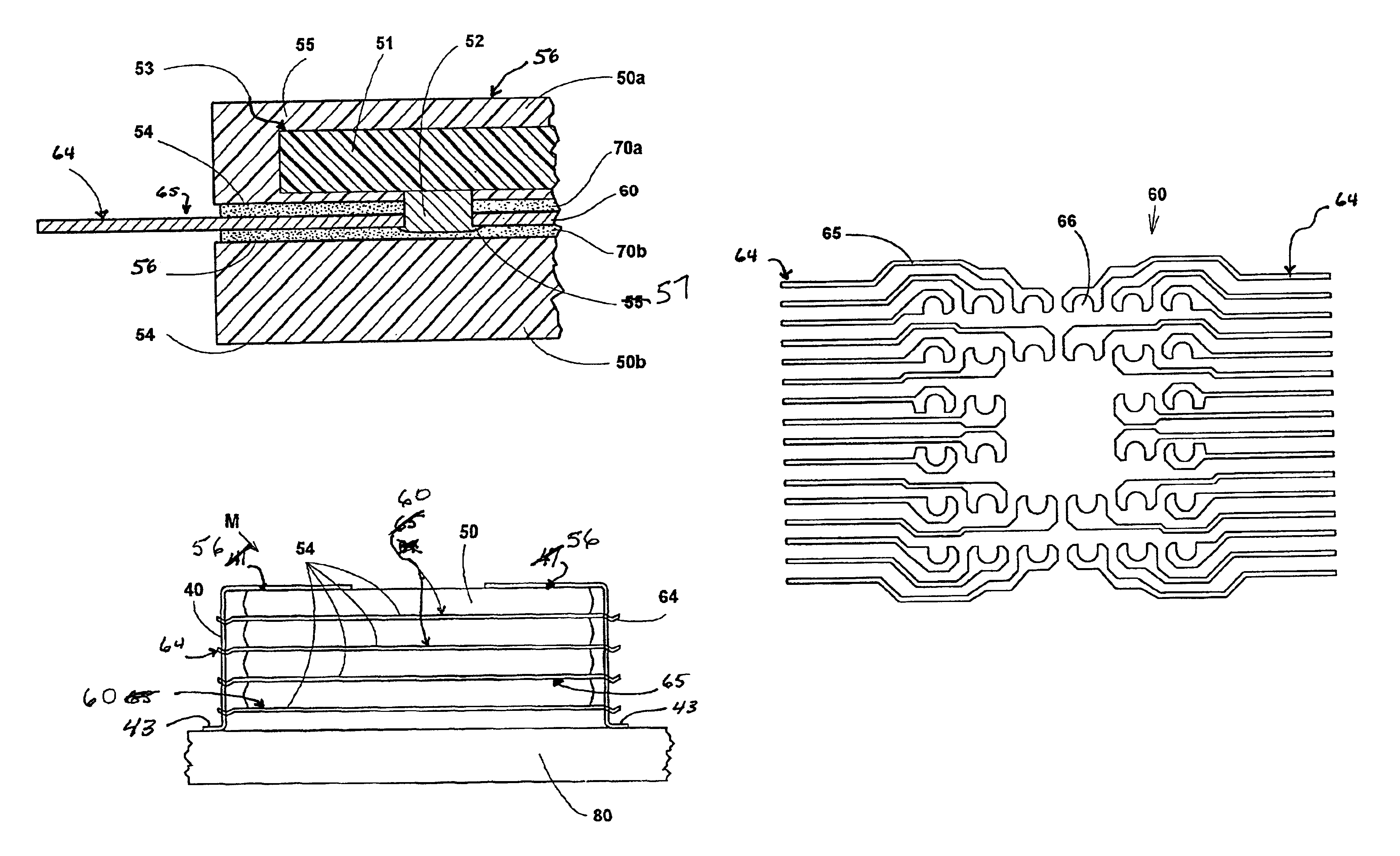
[0008]
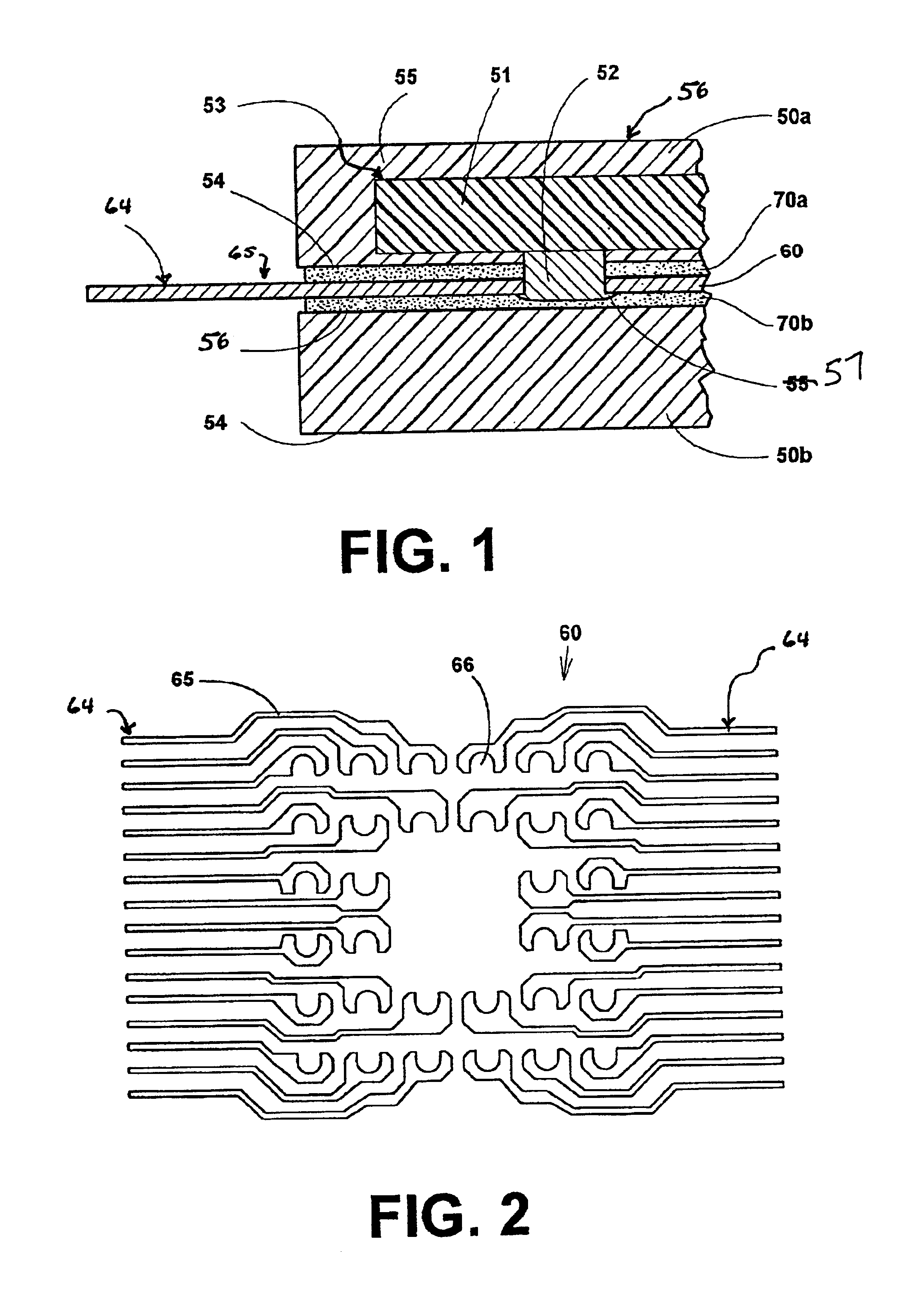
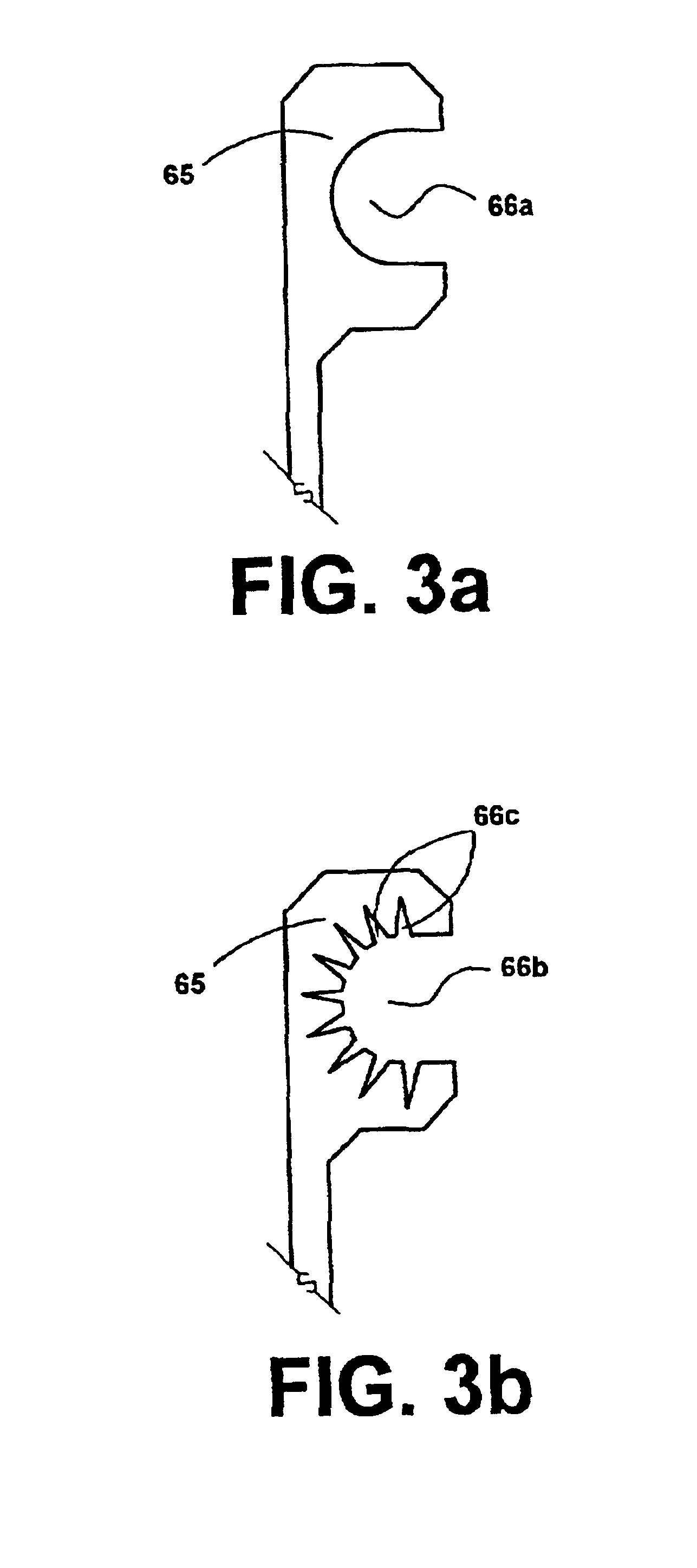
Connectivity to the leads of individual packages in a module is provided by thin substantially planar lead carriers located between adjacent packages. Lead carriers are adhered to adjacent packages with a thermally conductive but electrically insulating
adhesive. A lead carrier is comprised of elongated electrically and thermally conductive elements formed in one or more thin planes of conductive material that are separated by high-
dielectric material. Typically, each conductive element has at least one aperture, adapted to receive and electrically couple to an individual package ball and at least one interconnect lead that extends away from the module to provide
external circuit connectivity to package leads. Preferably, the lead carriers are formed from custom
flexible circuits commercially available from 3M™ or other manufacturers. These well known
flexible circuits are typically comprised of one or more thin
layers of conductive material that are die
cut and drilled to form ground planes,
signal traces, pads and apertures. The conductive layers are typically embedded in and between electrically-insulating, high-
dielectric material such as
polyamide,
polyester or teflon which results in circuits that are flexible, have dense trace, and provide accurate
impedance control.
[0010]Another object of the present invention is to provide an
assembly which effectively dissipates heat generated during normal operation. Efficient thermal management increases the operational life of the module, and improves reliability by eliminating the effects of elevated temperature on the electrical characteristics of the integrated circuit and packaging. When packages are not stacked, heat from the embedded integrated circuits, generated through normal operation, is primarily dissipated by
convection from the package's external surfaces to the surrounding air. When modules are formed by stacking packages, the buried packages have reduced surface area exposed to the air. The use of thermally conductive
adhesive facilitates the transmission of heat between adjacent packages and is an
effective method of taking
advantage of the exposed surfaces for removing heat from buried packages.
[0011]In the module of the present invention, the package leads are thermally coupled to the lead carrier and provide a path for heat from the embedded integrated circuits. Thermally conductive adhesive also facilitates transfer of heat from packages to the lead carrier.
[0012]In applications where it is desirable to reduce the package and module height, or where package or module warping is a concern, each package may be constructed using any of the various techniques described in U.S. Pat. Nos. 5,369,056, 5,369,058 and 5,644,161, each of which is assigned to the common assignee of the present invention and incorporated herein by reference. These patents describe methods for constructing thin, durable packages and modules with enhanced heat dissipation characteristics and minimal warpage.

