Encapsulated electronics device with improved heat dissipation

a technology of electronic components and encapsulation, which is applied in the direction of semiconductor devices, semiconductor/solid-state device details, electrical devices, etc., can solve the problems of damage to the chips, difficult to achieve a device of high resonant frequency using this fabrication method, and the internal heat distribution of the filter chip can be a problem, so as to improve the heat dissipation of the encapsulated device

Active Publication Date: 2006-01-31
NOKIA CORP
View PDF10 Cites 250 Cited by
  • Summary
  • Abstract
  • Description
  • Claims
  • Application Information

AI Technical Summary

Benefits of technology

[0021]providing a thermal conducting layer on the cleared area, so as to improve heat dissipation of the encapsulated device through the thermal conducting layer.

Problems solved by technology

In general, it is difficult to achieve a device of high resonant frequency using this fabrication method.
Over time, water vapor can penetrate the laminate 40 to cause damages to the chips.
In typical FBAR filters, especially under high power levels, the internal heat distribution inside the filter chip can be a problem.
The uneven internal heat distribution limits the highest usable power level with the FBAR filter or duplexer.
In particular, when the FBAR filters and duplexers are disposed in an encapsulated package, heat dissipation is a major concern.

Method used


Image

  • Encapsulated electronics device with improved heat dissipation
  • Encapsulated electronics device with improved heat dissipation
  • Encapsulated electronics device with improved heat dissipation

Examples


Embodiment Construction

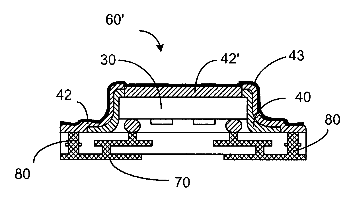
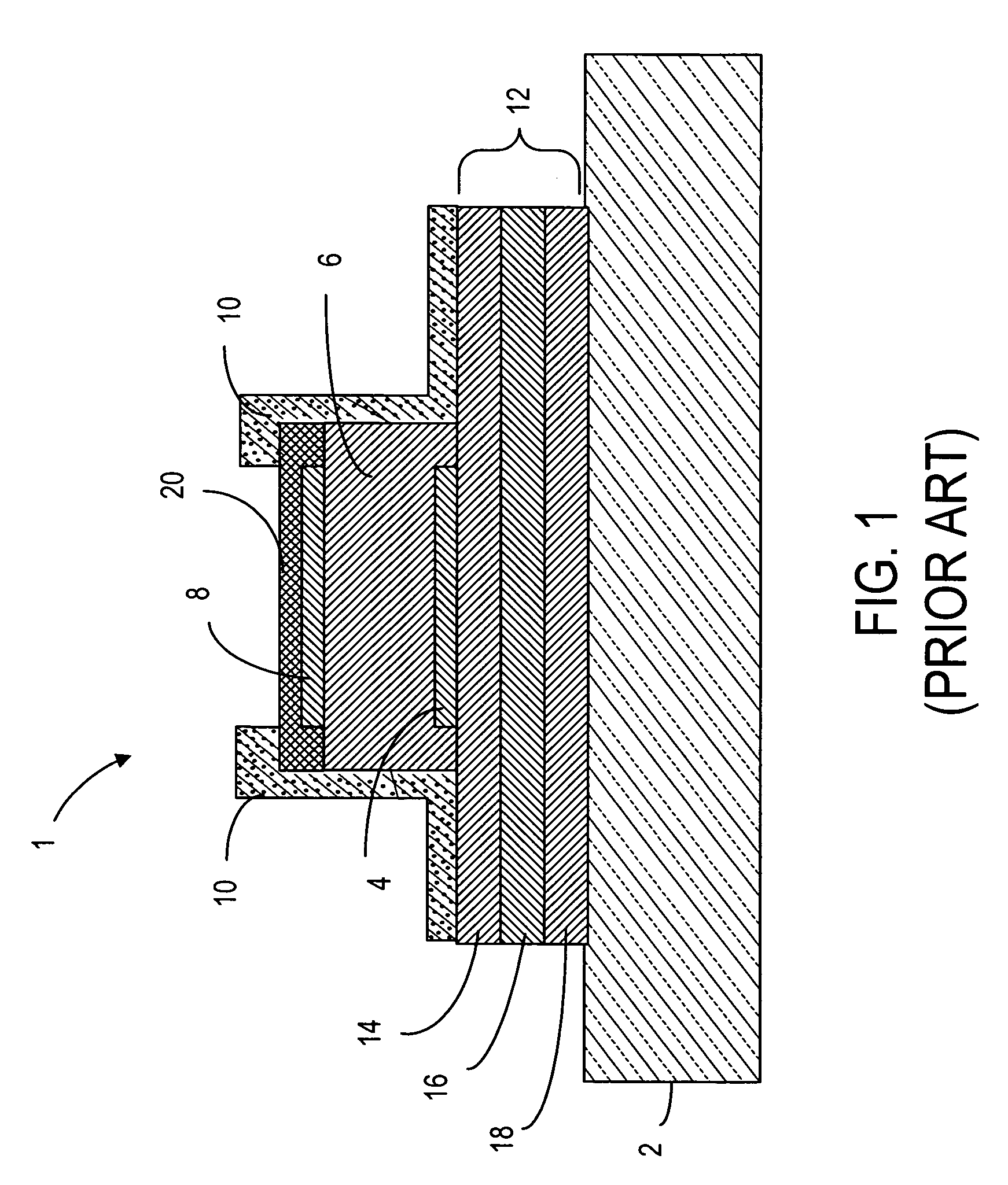
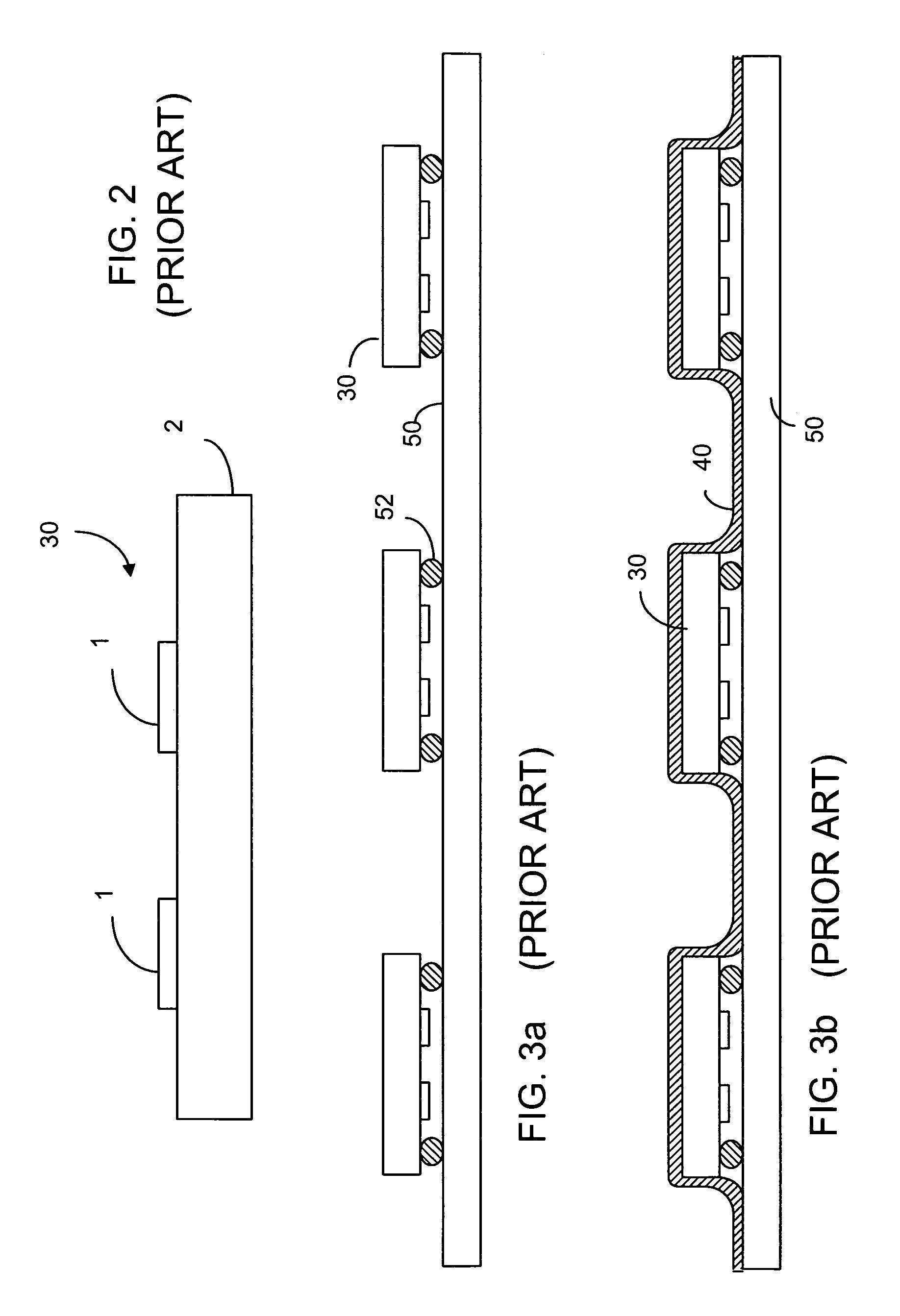
[0054]In an encapsulated package, such as the chip-size SAW package (CSSP) shown in FIG. 4, the heat produced inside the encapsulated package can be partly dissipated through the laminate 40 and the hermetic seal layer 42, and partly through the carrier 50 and the interconnecting vias 54. The laminate 40 is usually made of polyimide. In a typical CSSP, the laminate is about 40 μm thick in order to provide adequate mechanical protection for the electronic components in the package. The hermetic seal layer 42 is usually very thin coating of copper, about 10 μm. This hermetic seal layer itself is not sufficient to provide adequate mechanical protection. Furthermore, without the laminate, the thin copper layer cannot be directly deposited on top of the package to seal off the gap between the die 30 and the upper surface of the package carrier 50. The laminate 40 provides a smoother transition from the die 30 to the upper surface of the carrier 50. However, the laminate 40 is a poor ther...


PUM


Abstract

A method for improving heat dissipation in an encapsulated electronic package usually referred to as a chip-size SAW package. The package comprises one or more acoustic-wave components fabricated on a die, which is disposed on an electrically non-conductive carrier separated by electrically conducting bumps. The top of the package is covered by a laminate and a hermetic seal layer. Heat dissipation can be improved by removing a part of the laminate and then depositing a layer of thermal conducting material on the package, and by providing one or more heat conducting paths through the carrier.

Description

[0001]The invention claimed herein was made by or on behalf of EPCOS AG and Nokia Corporation through its wholly owned subsidiary NOKIA MOBILE PHONES LTD who are parties to a joint research agreement signed by EPCOS on Jan. 4, 2001 and by NOKIA MOBILE PHONES LTD on Jan. 19, 2001 relating at least to the field of the invention as described immediately below.FIELD OF THE INVENTION[0002]The present invention relates generally to encapsulated electronic components and, more particularly, to chip-size SAW package.BACKGROUND OF THE INVENTION[0003]It is known that a bulk acoustic-wave (BAW) device is, in general, comprised of a piezoelectric layer sandwiched between two electronically conductive layers that serve as electrodes. When a radio frequency (RF) signal is applied across the device, it produces a mechanical wave in the piezoelectric layer. The fundamental resonance occurs when the wavelength of the mechanical / acoustic wave (produced by the RF signal) is about twice the thickness o...

Claims


Application Information

Patent Timeline
Patent Type & Authority Patents(United States)
IPC IPC(8): H01L23/28H01L21/60H01L23/31H01L23/36H03H9/10
CPCH01L23/3135H03H9/1078H03H9/1085H01L24/97H01L2224/16227H01L2224/81801H01L2924/01057H01L2924/01079H01L2924/09701H01L2924/3011H01L2224/16225H01L2224/73204H01L2224/97H01L2924/01055H01L24/81H01L2924/01029H01L2224/81H01L2924/12042H03H2003/025H03H9/02102H01L2924/00H01L23/28H01L23/367H01L23/36H01L23/34
Inventor TIKKA, PASISCHMIDHAMMER, EDGARHEINZE, HABBOWELZER, REINERZIDEK, HERBERTSCHAUFELE, ANSGARELLA, JUHA
Owner NOKIA CORP
Why Eureka
Try Eureka