Display device substrate, display device, and related fabrication method

a technology of display device and substrate, which is applied in the direction of identification means, electrical apparatus casings/cabinets/drawers, instruments, etc., can solve the problems of non-uniform surface portions, substantial affecting the quality and/or stability of display device, and etc., to achieve satisfactory stability, reduce the non-uniform surface portions of display device substrate, and improve the quality of image display.

Inactive Publication Date: 2015-01-15
SAMSUNG DISPLAY CO LTD
View PDF37 Cites 4 Cited by
  • Summary
  • Abstract
  • Description
  • Claims
  • Application Information

AI Technical Summary

Benefits of technology

[0007]This cutting process may involve using a cutting means, for example, a knife, and may result in non-uniform surface portions of the display device substrate. The non-uniform surface portions may be cut surfaces and / or surface portions adjacent to cut surfaces and may have non-uniform molecular structures. Embodiments of the invention may minimize non-uniform surface portions of display device substrates. Advantageously, satisfactory stability, durability, impact resistance, and / or image display quality of display devices may be provided.

Problems solved by technology

The substrate(s) of a display device may substantially affect the quality and / or stability of the display device.
This cutting process may involve using a cutting means, for example, a knife, and may result in non-uniform surface portions of the display device substrate.
The non-uniform surface portions may be cut surfaces and / or surface portions adjacent to cut surfaces and may have non-uniform molecular structures.

Method used


Image

  • Display device substrate, display device, and related fabrication method
  • Display device substrate, display device, and related fabrication method
  • Display device substrate, display device, and related fabrication method

Examples


Embodiment Construction

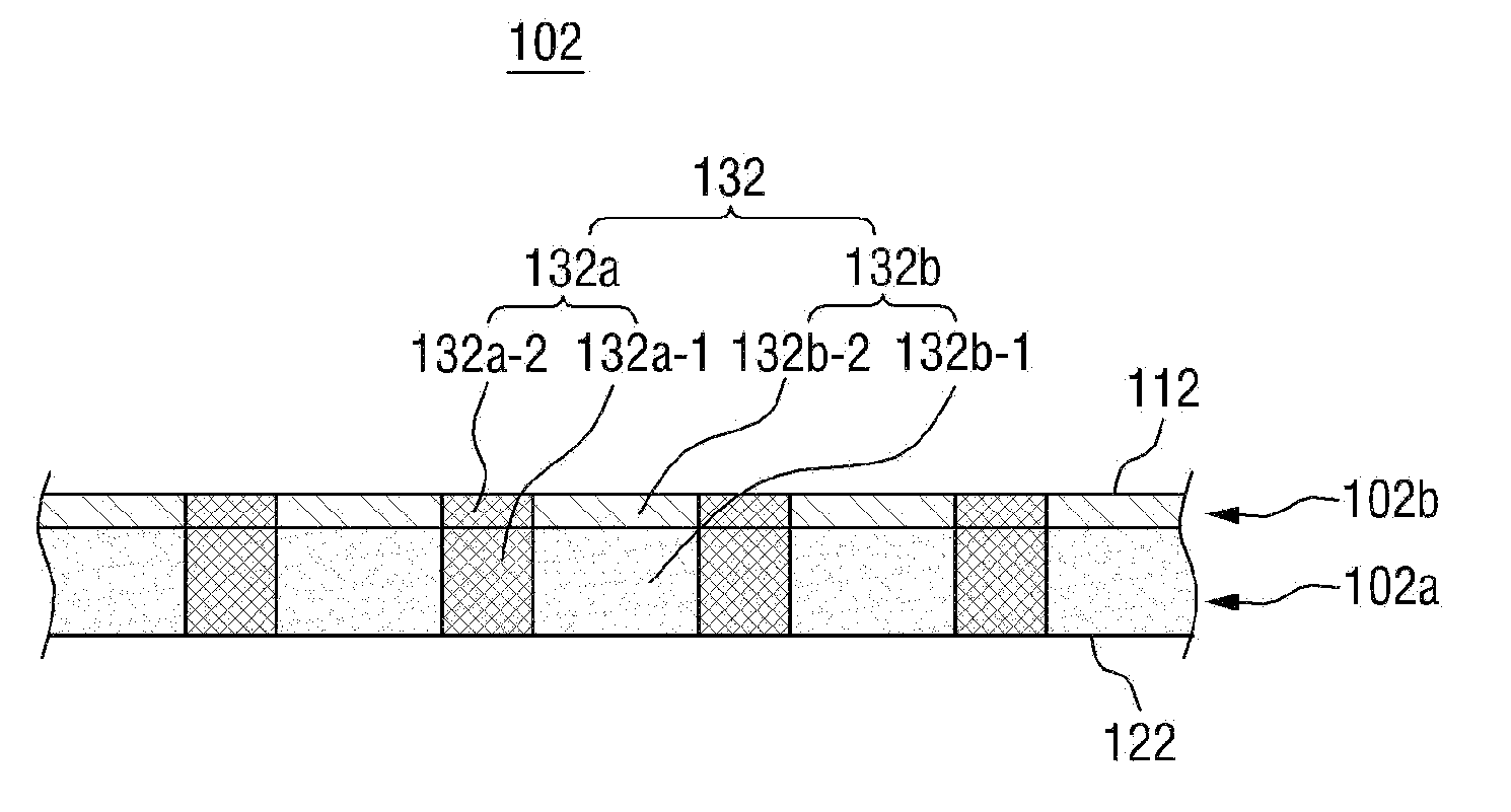
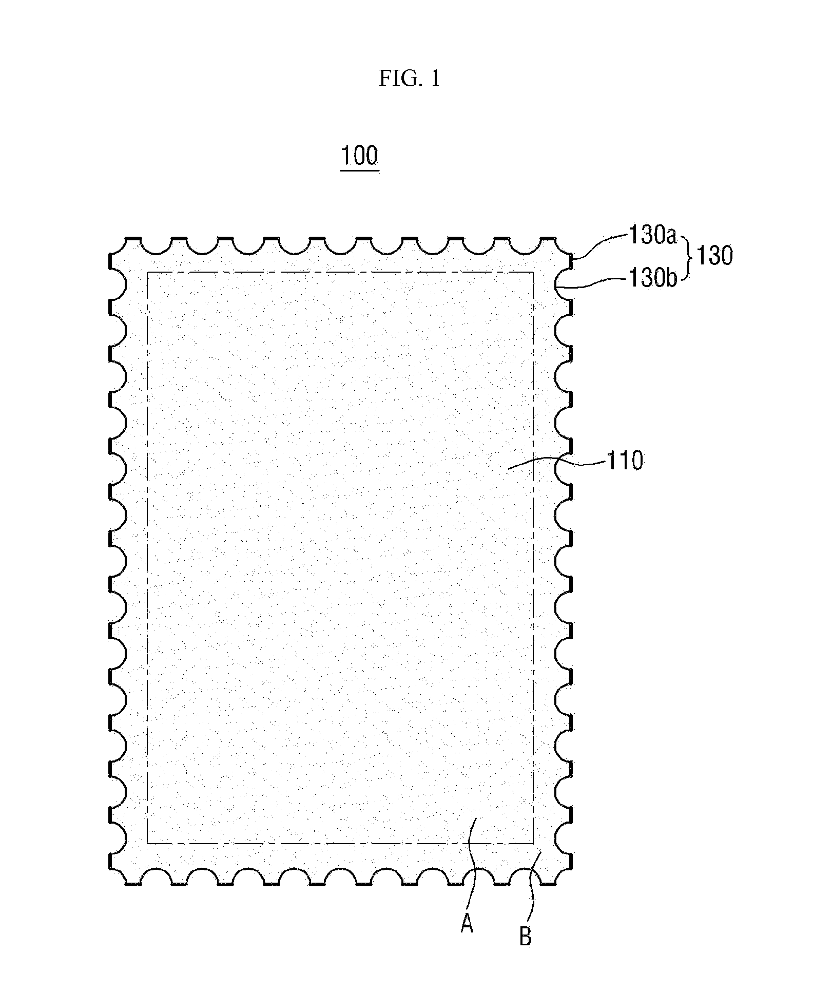
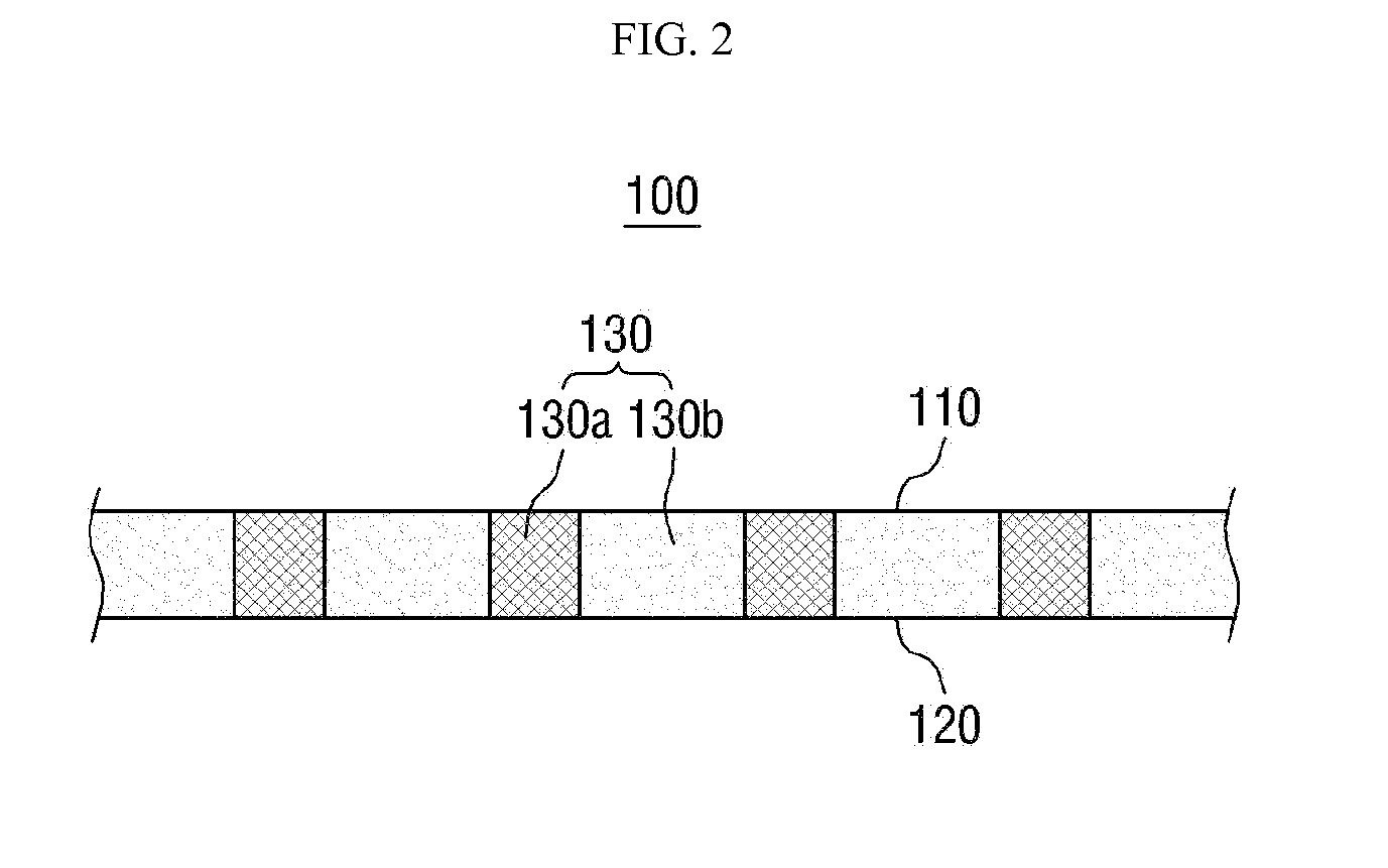
[0062]Embodiments of the present invention are described in detail with reference to the accompanying drawings. The present invention is not limited to the described embodiments, but can be implemented in various ways.

[0063]In the description and the drawings, the same reference numerals may indicate identical elements or analogous elements.

[0064]Although the terms “first”, “second”, and so forth” may be used to describe different elements, these elements are not limited by the terms. The terms are used to distinguish an element from one or more other constituent elements. Accordingly, in the following description, a first element may be called a second element. The description of an element as a “first” element may not require or imply the presence of a second element or other elements. The terms “first”, “second”, etc. may also be used herein to differentiate different categories of elements. For conciseness, the terms “first”, “second”, etc. may represent “first-type (or first-ca...


PUM

PropertyMeasurementUnit
glass transition temperatureaaaaaaaaaa

Abstract

A substrate is for use in a display device. The substrate may include a plurality of non-uniform surface portions, the non-uniform surface portions being spaced from each other and including a first non-uniform surface portion and a second non-uniform surface portion. The substrate may further include a plurality of substantially uniform surface portions having a molecular structure that is more uniform than a molecular structure of the plurality of non-uniform surface portions, the substantially uniform surface portions being spaced from each other and including a first substantially uniform surface portion that abuts each of the first non-uniform surface portion and the second non-uniform surface portion.

Description

CROSS-REFERENCE TO RELATED APPLICATIONS[0001]This application claims priority to and benefit of Korean Patent Application No. 10-2013-0077182, filed on Jul. 2, 2013 in the Korean Intellectual Property Office, the disclosure of which is incorporated herein in its entirety by reference.BACKGROUND[0002]1. Field of the Invention[0003]The present invention relates to a substrate, a display device that includes the substrate, and a method for fabricating the substrate.[0004]2. Description of the Prior Art[0005]A display device, such as a liquid crystal display, an electrophoretic display, an organic light emitting display, a FED (Filed Emission Display), a SED (Surface-conduction Electron-emitter Display), a plasma display, or a cathode ray tube display, typically includes at least one substrate that supports other components of the display device. The substrate(s) of a display device may substantially affect the quality and / or stability of the display device.SUMMARY[0006]In order to fabr...

Claims


Application Information

Patent Timeline
Patent Type & Authority Applications(United States)
IPC IPC(8): G06F1/16
CPCY10T428/24479G06F1/16Y10T428/24488G02F1/133351Y10T83/04G09F9/00
Inventor CHOI, JIN WOO
Owner SAMSUNG DISPLAY CO LTD
Why Eureka
Try Eureka