Switch module

a switch module and switch technology, applied in the field of switch modules, can solve problems such as the degradation of the characteristics of the front-end circuit fec, and achieve the effect of preventing the degradation of the characteristics of the switch module and significantly reducing or preventing the generation of undeired coupling within the common-terminal-side circui

Active Publication Date: 2015-03-05
MURATA MFG CO LTD
View PDF1 Cites 7 Cited by
  • Summary
  • Abstract
  • Description
  • Claims
  • Application Information

AI Technical Summary

Benefits of technology

[0024]According to various preferred embodiments of the present invention, the inner-layer ground electrode closest to the first circuit device is not superposed with the first circuit device when viewed in plan in the stacking direction of the multilayer substrate. Hence, the occurrence of the common-terminal-side circuit being coupled to the switching-terminal-side circuit through the inner-layer ground electrode is significantly reduced or prevented. Further, generation of undesired coupling within the common-terminal-side circuit is significantly reduced or prevented. As a result, degradation in the characteristics of the switch module is prevented.

Problems solved by technology

These couplings, which degrade isolation characteristics among the chip devices, cause degradation in the characteristics of the front-end circuit FEC.

Method used


Image

  • Switch module
  • Switch module
  • Switch module

Examples


first preferred embodiment

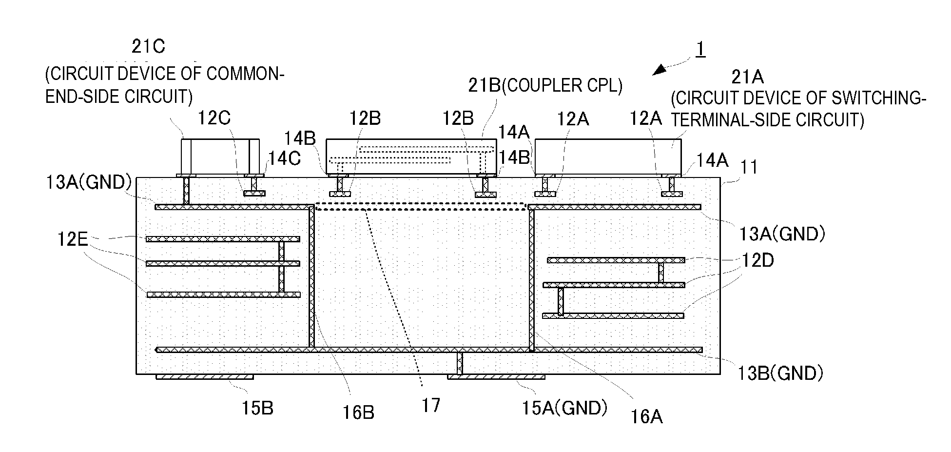
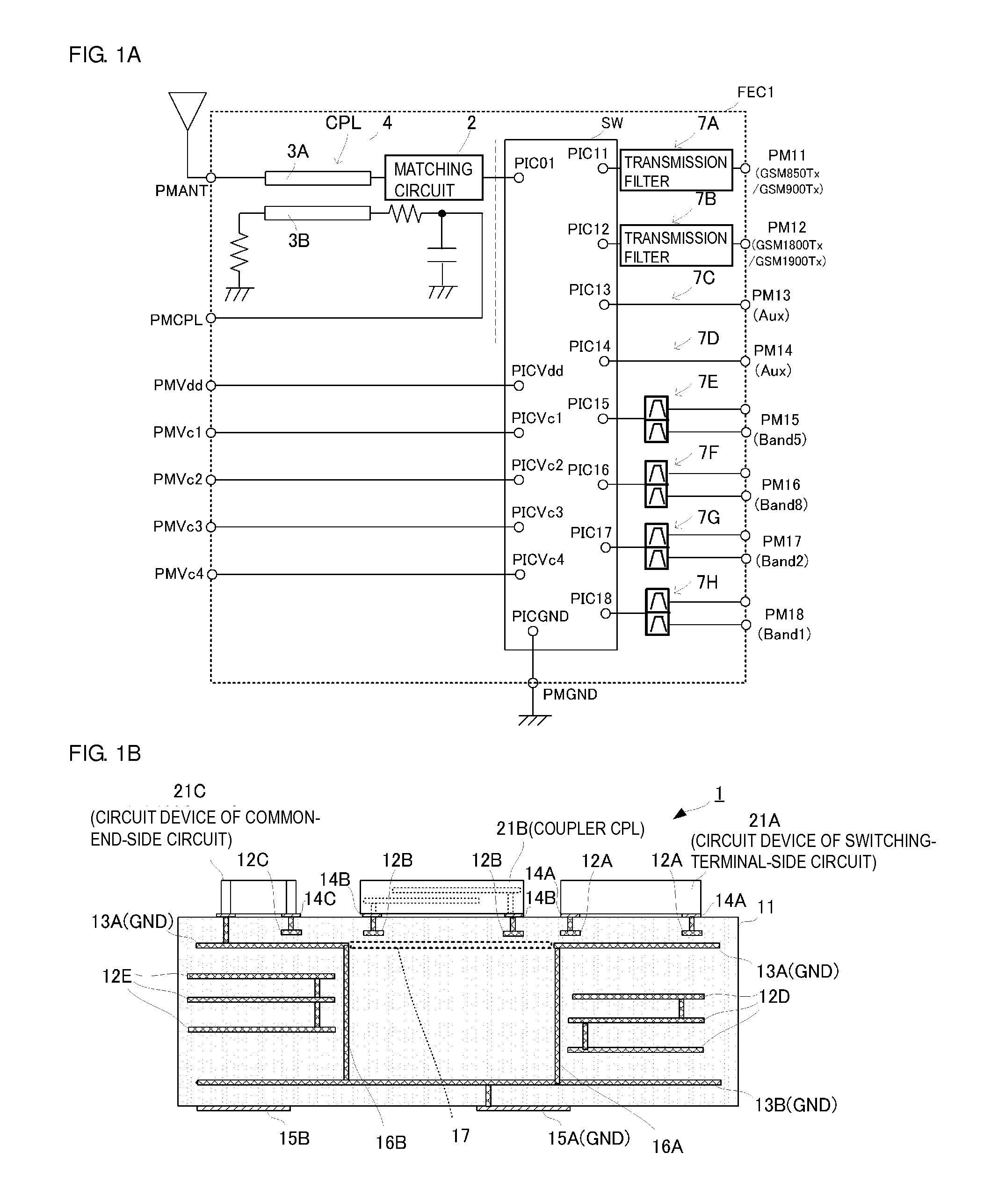
[0038]Hereinafter, a switch module according to a first preferred embodiment of the present invention will be described with reference to FIG. 1A to FIG. 1D.

[0039]FIG. 1A is a block diagram illustrating the circuit configuration of a first preferred embodiment of the present invention. A front-end circuit FEC1 illustrated in FIG. 1A includes a switch circuit SW, a common-terminal-side circuit 4, and switching-terminal-side circuits 7A to 7H.

[0040]The switch circuit SW includes a power supply port PICVdd, control ports PICVc1 to PICVc4, a common port PIC01, and switching ports PIC11 to PIC18. The power supply port PICVdd is a port to which a driving voltage of the switch circuit SW is applied. The control ports PICVc1-PICVc4 are ports to which respective control voltages are applied. The common port PIC01 is a port corresponding to the common terminal in the present preferred embodiment. The switching ports PIC11 to PIC18 are ports corresponding to the switching terminals in the pres...

second preferred embodiment

[0083]Hereinafter, a switch module according to a second preferred embodiment of the present invention will be described with reference to FIG. 2A and FIG. 2B.

[0084]FIG. 2A is a block diagram illustrating the circuit configuration of a switching module according to the present preferred embodiment. A front-end circuit FEC2 illustrated in FIG. 2A includes a switch circuit SW, a common-terminal-side circuit 4, and switching-terminal-side circuits 7A to 7H. Note that the internal configurations of the switch circuit SW, the common-terminal-side circuit 4, and the switching-terminal-side circuits 7A and 7B are preferably the same as those of the front-end circuit FEC1 according to the first preferred embodiment and, hence, the descriptions thereof are omitted here. The front-end circuit FEC2 has a configuration in which the duplexers have been removed from the front-end circuit FEC1 of the first preferred embodiment and the switching-terminal-side circuits 7C to 7H include transmission ...

third preferred embodiment

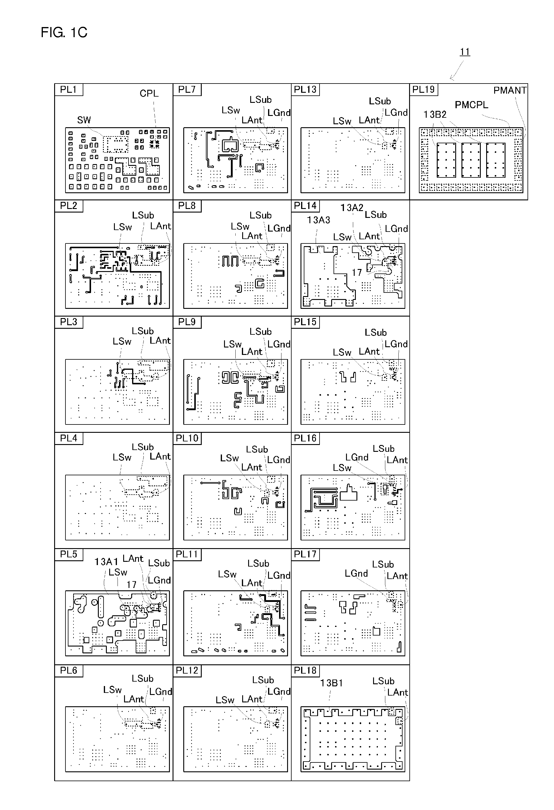
[0106]Hereinafter, a switch module according to a third preferred embodiment of the present invention will be described with reference to FIG. 3. Note that a block diagram illustrating the circuit configuration of the switch module according to the present preferred embodiment is preferably the same as that of the front-end circuit FEC1 and, hence, description thereof is omitted here. Further, the schematic diagram of the cross-sectional configuration of the switch module according to the present preferred embodiment is preferably the same as that of the switch module 1 according to the first preferred embodiment and, hence, description thereof is omitted here.

[0107]FIG. 3 is a stacking diagram illustrating a multilayer substrate 31 of an example of the switch module according to the third preferred embodiment of the present invention. The multilayer substrate 31 illustrated here preferably includes 19 layers of ceramic layers (dielectric layers) stacked on top of one another. In th...


PUM

PropertyMeasurementUnit
areaaaaaaaaaaa
frequencyaaaaaaaaaa
cross-sectional structureaaaaaaaaaa

Abstract

A switch module includes a switch circuit, a chip device which is a coupler, a chip device that defines together with the coupler a common-terminal-side circuit, chip devices defining switching-terminal-side circuits, and a multilayer substrate. The multilayer substrate includes inner-layer ground electrodes. A first inner-layer ground electrode is closer to the chip device than a second inner-layer ground electrode and includes an opening arranged so as not to be superposed with the chip device when viewed in plan in the stacking direction of the multilayer substrate.

Description

BACKGROUND OF THE INVENTION[0001]1. Field of the Invention[0002]The present invention relates to a switch module configured to receive and transmit a plurality of communication signals using a common antenna.[0003]2. Description of the Related Art[0004]In recent years, a communication apparatus has come to transmit and receive a plurality of communication signals in different frequency bands using a common antenna, as cellular phones and the like have come to use multiple bands (refer to, for example, Japanese Unexamined Patent Application Publication No. 2008-10995). As a result, a communication apparatus has increasingly utilized a switch module that connects a plurality of communication circuits to a common antenna through switching.[0005]FIG. 6A is a block diagram illustrating a general circuit configuration of a switch module.[0006]A front-end circuit FEC illustrated in FIG. 6A includes a switch circuit SW, a common-terminal-side circuit 104, and switching-terminal-side circuit...

Claims


Application Information

Patent Timeline
Patent Type & Authority Applications(United States)
IPC IPC(8): H05K1/18
CPCH05K1/18H01L2223/6677H01L2224/16227H01L2924/15313H01L2924/19105H04B1/0057H05K1/0215H05K1/0298H05K2201/10098
Inventor ONO, ATSUSHIUEJIMA, TAKANORI
Owner MURATA MFG CO LTD
Why Eureka
Try Eureka