Method of manufacturing a semiconductor device

a manufacturing method and semiconductor technology, applied in semiconductor/solid-state device manufacturing, basic electric elements, electric devices, etc., can solve the problems of electrical characteristics degradation, reliability and productivity of semiconductor devices, and the inability to fully remove the oxide layer easily, so as to prevent the degradation of electrical characteristics

Inactive Publication Date: 2006-06-29
DONGBU ELECTRONICS CO LTD
View PDF15 Cites 3 Cited by
  • Summary
  • Abstract
  • Description
  • Claims
  • Application Information

AI Technical Summary

Benefits of technology

[0012] The present invention has been made in an effort to provide a method of manufacturing a semiconductor device having advantages of preventing degradation of electrical characteristics of a semiconductor device by fully removing a residue such as a polymer formed in a trench.

Problems solved by technology

Such a polymer formed in the trench during the etching process of the oxide layer may not be fully removed easily by a dry ashing process or a solvent cleaning process, and it frequently remains in the trench.
However, a crown defect formed in the trench may be a cause of degradation of electrical characteristics of a metal material that will be filled in the via hole and the trench.
In this case, the reliability and productivity of the semiconductor device may deteriorate.

Method used


Image

  • Method of manufacturing a semiconductor device
  • Method of manufacturing a semiconductor device
  • Method of manufacturing a semiconductor device

Examples


Embodiment Construction

[0023] An exemplary embodiment of the present invention will hereinafter be described in detail with reference to the accompanying drawings.

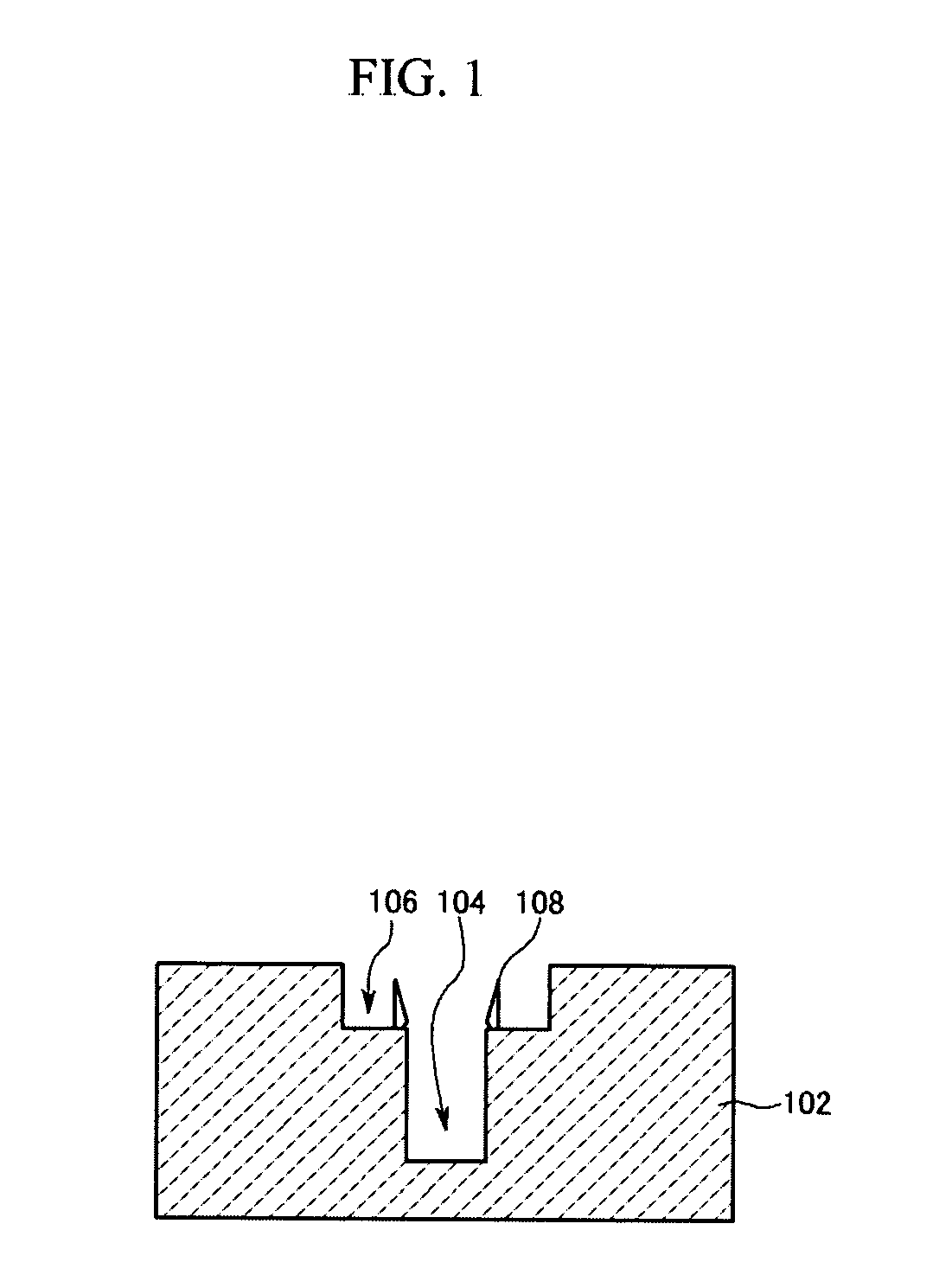
[0024] According to an exemplary embodiment of the present invention, after a via hole and a trench are formed on or in a semiconductor substrate, a photoresist is formed entirely (e.g., blanket deposited) thereon, and then the photoresist is partially removed (e.g., by photolithography and development). Accordingly, a polymer residue (for example, a crown defect) may be exposed. After the exposed polymer residue is removed, the photoresist remaining in the via hole and the trench is removed by a plasma treatment. As a result, the trench may be free from a polymer residue.

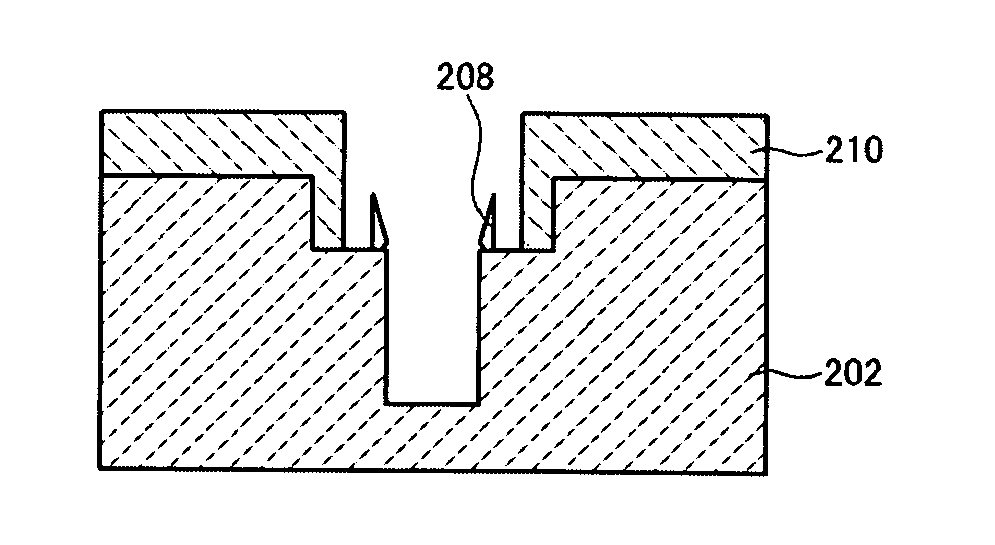
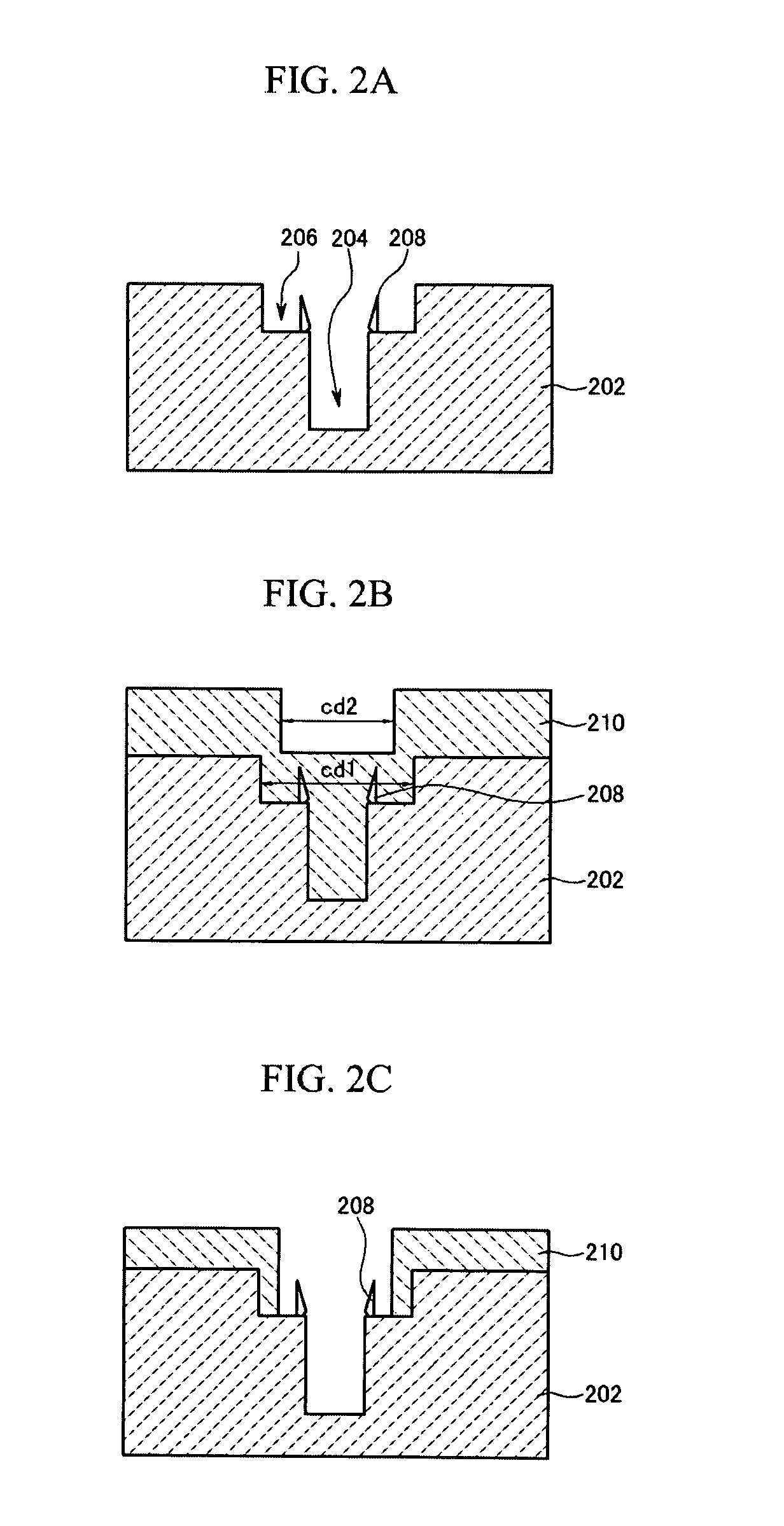
[0025]FIG. 2A to FIG. 2E are cross-sectional views showing sequential stages of forming a trench on a semiconductor substrate by an etching process according to an exemplary embodiment of the present invention.

[0026] Referring to FIG. 2A, a photoresist pattern is formed on a...


PUM


Abstract

Electrical characteristics of a semiconductor device may be enhanced by completely removing a residue such as a polymer formed in a trench when the semiconductor device is manufactured by a method including: forming a via hole and a trench on a semiconductor substrate by an etching process; coating a photoresist on an entire surface of the semiconductor substrate such that the via hole and the trench may be filled thereby; removing a polymer defect in the trench while removing the coated photoresist by a plasma treatment under predetermined process conditions; and performing a wet cleaning process so as to remove a residue of the photoresist.

Description

CROSS-REFERENCE TO RELATED APPLICATION [0001] This application claims priority to and the benefit of Korean Patent Application No. 10-2004-0113659, filed in the Korean Intellectual Property Office on Dec. 28, 2004, the entire contents of which are incorporated herein by reference. BACKGROUND OF THE INVENTION [0002] (a) Field of the Invention [0003] The present invention relate to a method of manufacturing a semiconductor device. More particularly, the present invention relates to a method of manufacturing a semiconductor device that removes residues of polymer remaining in a trench for a metal line. [0004] (b) Description of the Related Art [0005] Typically, a semiconductor device has a plurality of layers sequentially formed on a substrate. In such a multi-layered structure, an interlayer insulation layer such as an oxide layer is required for insulation between layers, and a metal line may be formed in each layer. [0006] Accordingly, metal lines (i.e., upper and lower metal lines)...

Claims


Application Information

Patent Timeline
Patent Type & Authority Applications(United States)
IPC IPC(8): H01L21/4763H01L21/302
CPCH01L21/02063H01L21/31138H01L21/76807H01L21/76814H01L21/28
Inventor JO, BO-YEOUN
Owner DONGBU ELECTRONICS CO LTD
Why Eureka
Try Eureka