

Field-effect transistor
a field-effect transistor and transistor technology, applied in the field of field-effect transistors, can solve the problems of deteriorating electric characteristics of field-effect transistors, crystal defects, and deterioration of field-effect transistor characteristics, and achieve the effect of preventing deterioration of electric characteristics
- Summary
- Abstract
- Description
- Claims
- Application Information
AI Technical Summary
Benefits of technology
Problems solved by technology
Method used
Image

Examples
first embodiment
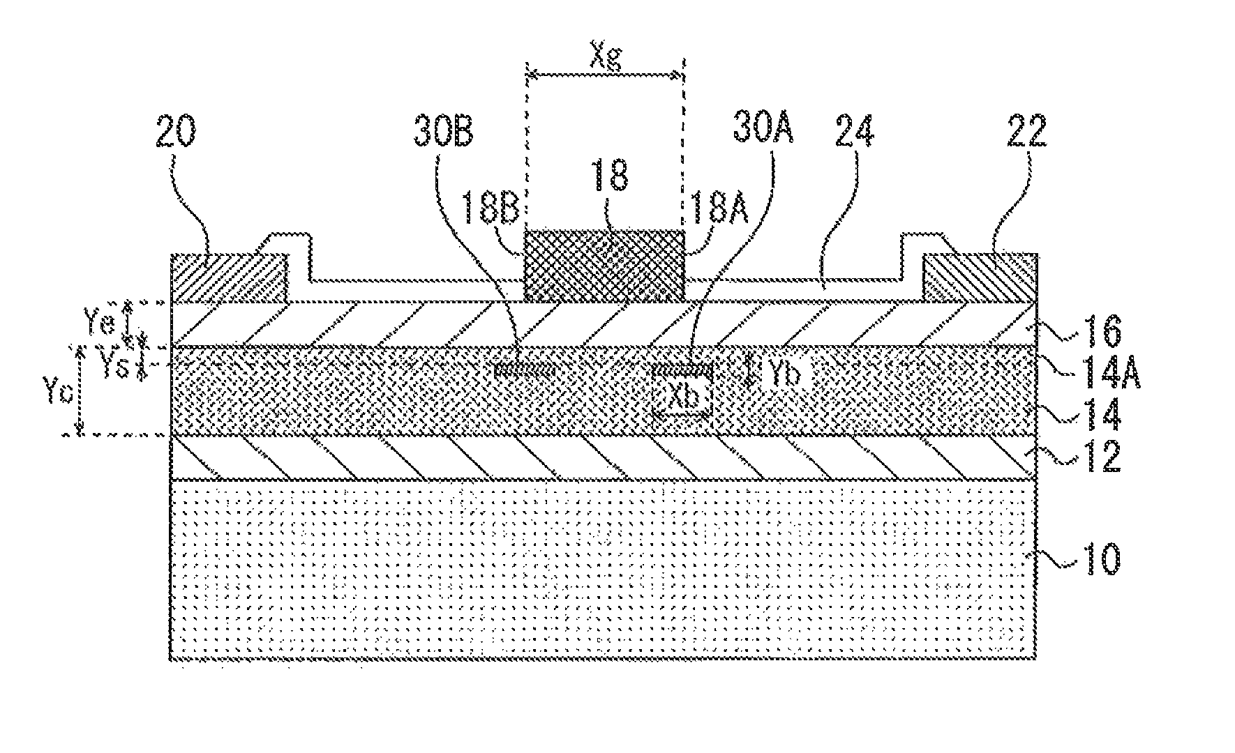
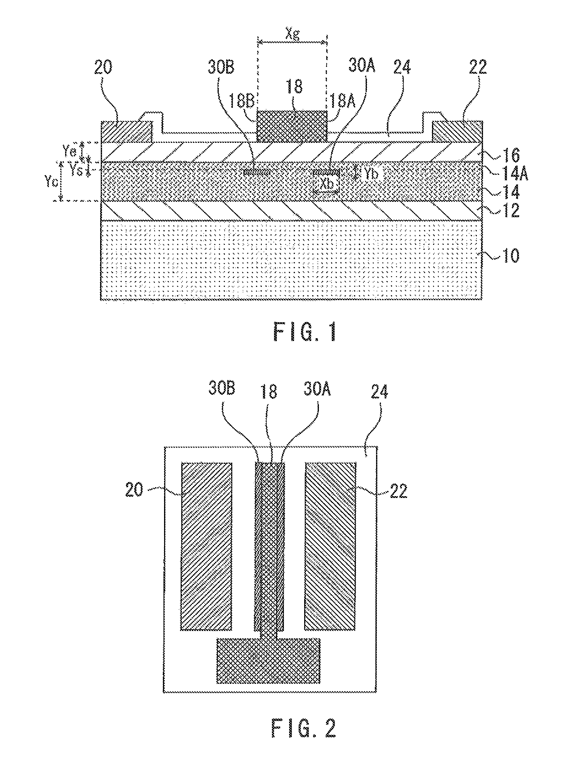
[0023]FIG. 1 is a cross-sectional view of a field-effect transistor according to a first embodiment of the present invention. This field-effect transistor is provided with a substrate 10 made of, for example, SiC or Si. A channel layer 14 is formed above the substrate 10 via a lattice relaxation layer 12. The lattice relaxation layer 12 is made of AIN to reduce a lattice mismatch between the substrate 10 and the channel layer 14. The channel layer 14 is made of GaN. A layer thickness Yc of the channel layer 14 is, for example, 1 μm. A two-dimensional electron gas (2DEG) is formed in the channel layer 14.
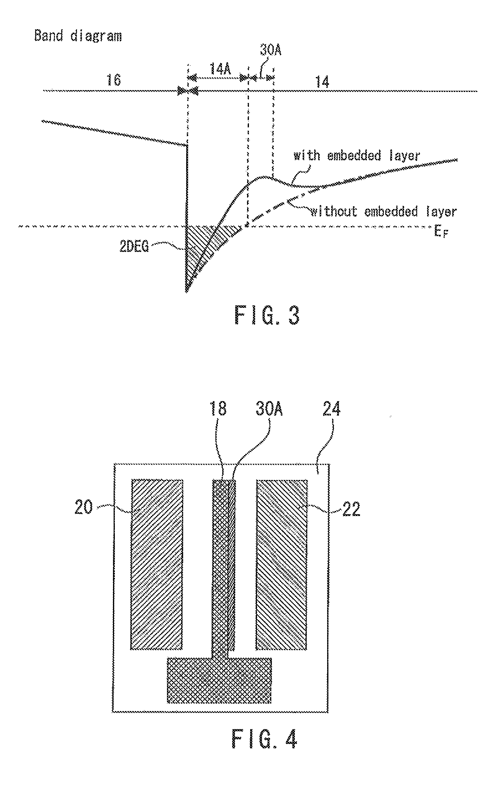
[0024]An electron supply layer 16 is formed on the channel layer 14. The electron supply layer 16 is made of AlGaN. The electron supply layer 16 has a layer thickness Ye of, for example, 20 to 30 nm. The electron supply layer 16 is a layer that forms a Schottky barrier and also supplies electrons to the channel layer 14. Note that the lattice relaxation layer 12, the channel layer 14...
second embodiment
[0036]Since a field-effect transistor according to a second embodiment of the present invention has many points in common with the first embodiment, differences from the first embodiment will be mainly described. FIG. 6 is a plan view of the field-effect transistor according to the second embodiment of the present invention. Embedded layers 30E are formed intermittently along the gate electrode 18 in a plan view. The same applies to additional embedded layers 30F.
[0037]According to the field-effect transistor according to the second embodiment of the present invention, by changing the sizes of the embedded layers 30E and the additional embedded layers 30F formed into an island shape, it is possible to easily adjust the potential of the two-dimensional electron gas region.
third embodiment
[0038]Since a field-effect transistor according to a third embodiment of the present invention has many points in common with the first embodiment, differences from the first embodiment will be mainly described. FIG. 7 is a cross-sectional view of the field-effect transistor according to the third embodiment of the present invention. An embedded layer 30G is embedded over the whole surface of a so-called active region of the channel layer 14.
[0039]According to the field-effect transistor according to the third embodiment of the present invention, it is possible to increase the potential of the whole two-dimensional electron gas region.
PUM
 Abstract
Description
Claims
Application Information