Electroluminescent display device

a technology of display device and electroluminescent light, which is applied in the direction of semiconductor devices, electrical devices, instruments, etc., can solve the problems of image quality and non-uniform luminan

Active Publication Date: 2019-05-30
LG DISPLAY CO LTD
View PDF0 Cites 17 Cited by
  • Summary
  • Abstract
  • Description
  • Claims
  • Application Information

AI Technical Summary

Benefits of technology

[0021]In another aspect, an electroluminescent display device comprises a display panel including a display area and a non-display area and including a plurality of pixel lines each including a plurality of pixel circuits. Also, each of the plurality of pixel circuits included in an nth pixel line of the plurality of pixel lines may include a driving transistor connected between a first node and a third node and including a gate connected to a second node, a first transistor allowing a current to flow between the second node and the third node in response to an nth scan signal, a second transistor applying a reference voltage to the first node in response to the nth scan signal, a third transistor applying a high-level power voltage to the first node in response to an nth emission signal, a fifth transistor applying an initialization voltage to a fourth node in response to the nth scan signal, a sixth transistor applying the high-level power voltage to a

Problems solved by technology

Some of compensation methods do not consider the drop of a source voltage applied to each subpixel, causing an image

Method used


Image

  • Electroluminescent display device
  • Electroluminescent display device
  • Electroluminescent display device

Examples


first embodiment

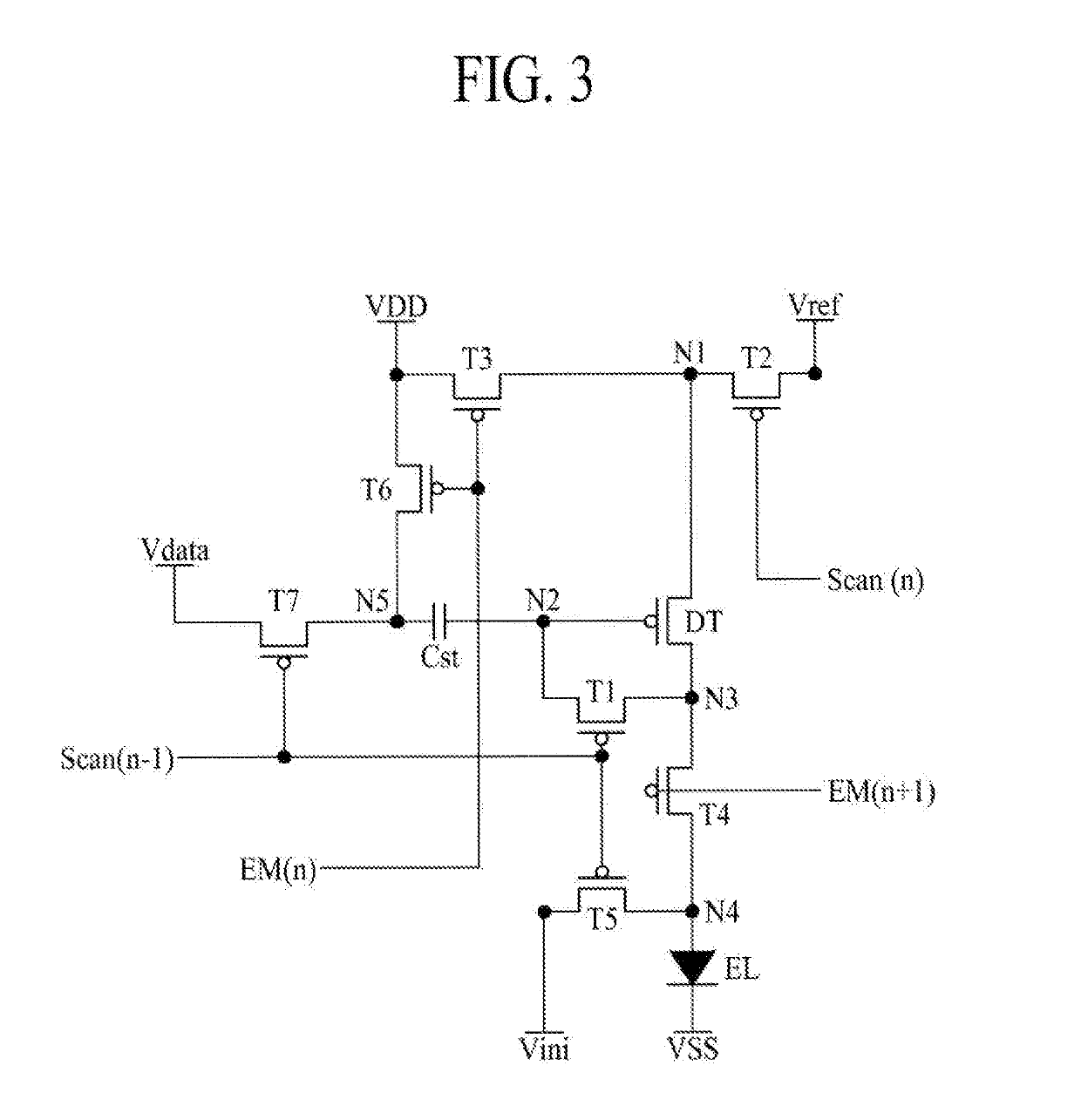
[0092]FIG. 3 is a circuit diagram of a subpixel SP according to the present disclosure.

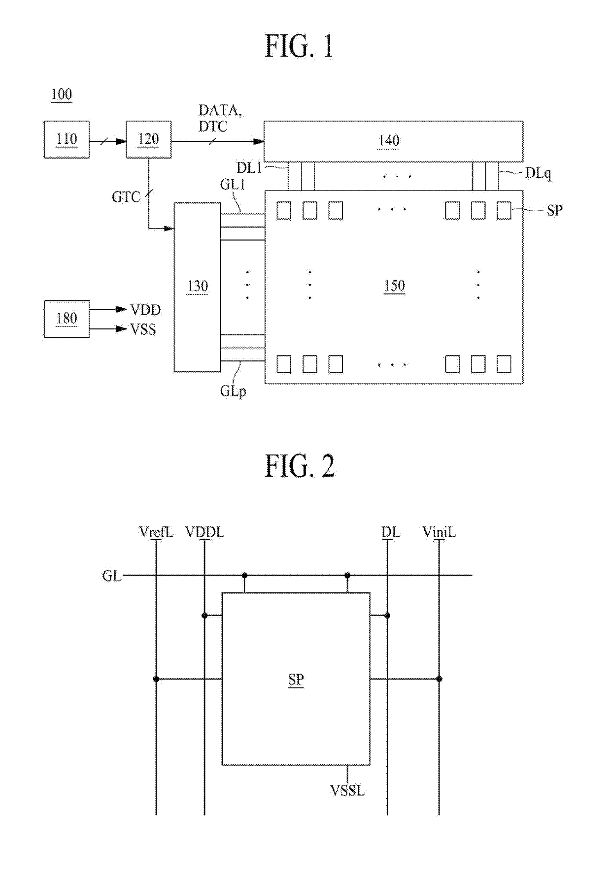
[0093]The display panel 150 may include the display area, which displays an image based on the subpixels SP and / or the first part of the pixel circuits, and the non-display DA area which does not display an image and where signal lines, driving circuits, the second part of the pixel circuits, and the like are disposed.

[0094]The electroluminescent display device 100 may display an image based on light emitted from a light emitting device EL included in each of the subpixels SP. However, in each subpixel SP, the voltage drop of a line to which a source voltage is applied occurs due to a sequential shift characteristic where a threshold voltage of an element included in each subpixel SP is shifted and enlarging of the display panel 150, and thus, it is required to compensate for the voltage drop.

[0095]Therefore, a pixel circuit which recognizes a problem causing an image quality issue such as vertica...

second embodiment

[0130]FIG. 9 is a circuit diagram of a subpixel according to the present disclosure. FIG. 9 is a modification example where one transistor is added to the pixel circuit of FIG. 3, and thus, overlapping descriptions are omitted or will be briefly described.

[0131]An nth subpixel SP according to a second embodiment of the present disclosure may include first to eighth transistors T1 to T8, a driving transistor DT, a capacitor Cst, and a light emitting device EL. In the second embodiment of the present disclosure, the nth subpixel SP may be implemented based on a total of nine transistors and one capacitor.

[0132]The driving transistor DT may include a source connected to a first node N1, a gate connected to a second node N2, and a drain connected to a third node N3. When a gate-on voltage is applied to the second node N2, the driving transistor DT may be turned on to provide a constant current to the third node N3.

[0133]The first transistor T1 may include a gate connected to an nth scan...

third embodiment

[0166]FIG. 14 is a circuit diagram of a subpixel according to the present disclosure. In comparison with FIG. 3, an eighth transistor T8 is added to the subpixel of FIG. 14, and the fourth transistor T4 illustrated in FIG. 3 is not applied to the subpixel of FIG. 14. FIG. 14 is a modification example which is implemented by modifying the pixel circuit of FIG. 3, and thus, overlapping descriptions are omitted or will be briefly described.

[0167]An nth subpixel SP may include first to third transistors T1 to T3, fifth to seventh transistors T5 to T7, a ninth transistor T9, a driving transistor DT, a capacitor Cst, and a light emitting device EL. In the third embodiment of the present disclosure, the nth subpixel SP may be implemented based on a total of eight transistors and one capacitor.

[0168]The driving transistor DT may include a source connected to a first node N1, a gate connected to a second node N2, and a drain connected to a third node N3. When a gate-on voltage is applied to ...


PUM


Abstract

Disclosed is an electroluminescent display device. The electroluminescent display device includes a display area and a non-display area. And the electroluminescent display device includes a display panel including a plurality of pixel lines each including a plurality of pixel circuits.

Description

CROSS-REFERENCE TO RELATED APPLICATIONS[0001]This application claims the benefit of the Korean Patent Applications No. 10-2017-0163682 filed on Nov. 30, 2017 and No. 10-2017-0163688 filed on Nov. 30, 2017, in the Korean Intellectual Property Office, the disclosure of which is incorporated herein by reference in its entirety.BACKGROUNDTechnical Field[0002]The present disclosure relates to an electroluminescent display device, and more particularly, to an electroluminescent display device including a pixel circuit for compensating a voltage drop.Discussion of the Related Art[0003]With the advancement of information-oriented technology, the market in display devices corresponding to a connection medium between a user and information is increasing. The use of various types of display devices such as electroluminescent display devices, liquid crystal display devices, and quantum dot display devices is increasing.[0004]In the electroluminescent display devices, when a gate signal, a data ...

Claims


Application Information

Patent Timeline
IPC IPC(8): G09G3/3258H01L27/32
CPCG09G2310/0243G09G2310/0264G09G3/3258H01L27/3276H01L27/3248G09G3/3233G09G2300/043G09G2300/0814G09G2300/0819G09G2320/0214G09G2320/0223H10K59/123H10K59/131
Inventor KIM, DONGHYUNYOO, JUHNSUKKIM, JUNGCHULJEONG, HAEYOONCHUNG, HOONJU
Owner LG DISPLAY CO LTD
Why Eureka
Try Eureka