Electroluminescent display panel having pixel driving circuit

a technology of pixel driving circuit and display panel, which is applied in the direction of electrical equipment, semiconductor devices, instruments, etc., can solve the problems of poor image quality such as stains, afterimages, cross-talk on the screen, etc., and achieve the effect of sufficient compensation tim

Active Publication Date: 2021-03-30
LG DISPLAY CO LTD
View PDF2 Cites 20 Cited by
  • Summary
  • Abstract
  • Description
  • Claims
  • Application Information

AI Technical Summary

Benefits of technology

[0008]The present disclosure is made in view of the above-mentioned problems and provides a pixel driving circuit which allows sufficient compensation time to be secured in high-resolution and high-frequency driving.
[0009]The present disclosure provides an electroluminescent display panel including a pixel driving circuit having improved response speed through high-speed driving and improved image quality through removal of spots, afterimages, and crosstalk from a screen by securing sufficient compensation time for compensating for a time-varying characteristic of a display panel.
[0010]The present disclosure provides an electroluminescent display panel including a pixel driving circuit having reduced bezel BZ by at least one of improving the degree of integration of the pixel driving circuit composed of a plurality of transistors, diversifying the types of the transistors, and simplifying circuits included in a gate driving circuit.
[0012]There is provided an electroluminescent display panel according to an aspect of the present disclosure in which each of a plurality of subpixels included in an nth row (here, n is a natural number) includes a pixel driving circuit that is driven according to or in an initialization period, a sampling period, a programming period, and an emission period, wherein the pixel driving circuit includes a light-emitting element, a first capacitor connected to a first node and a second node, a second capacitor connected to the second node and a high potential voltage line which provides a high potential voltage, a driving transistor configured to supply electric current to the light-emitting element and controlled by a voltage applied to the first node, a first switching circuit controlled by a first scan signal and turned on during the sampling period to compensate for a time-varying characteristic of the driving transistor, a second switching circuit controlled by a second scan signal and turned on during the programming period to apply a data voltage to the second node, and a light emission control circuit controlled by an emission signal and turned on during the initialization period and the emission period to apply the high potential voltage to the driving transistor. In this case, the sampling period is longer as one horizontal period or has a period exceeding one horizontal period, and the initialization period and the programming period are equal to one horizontal period. Thus, a sampling period can be provided for a high-resolution / high-frequency display panel which is sufficiently long, since usually in common high-resolution / high-frequency display panels the horizontal period is decreased. However, according to the present disclosure the sampling period may be sufficiently secured, and thus it is possible to improve an image quality of the display panel by enhancing compensation capability of a pixel driving circuit.
[0013]There is provided an electroluminescent display panel according to an aspect of the present disclosure in which each of a plurality of subpixels included in an nth row (here, n is a natural number) includes a pixel driving circuit that is driven according to an initialization period, a sampling period, a programming period, and a emission period, wherein the pixel driving circuit includes a light-emitting element, a first capacitor connected to a first node and a second node, a second capacitor connected to the second node and a high potential voltage line, a driving transistor configured to supply electric current to the light-emitting element and controlled by a voltage applied to the first node, a first switching circuit controlled by a first emission signal and turned on during the sampling period to compensate for a time-varying characteristic of the driving transistor, a second switching circuit controlled by a scan signal and turned on during the programming period to apply a data voltage to the second node, and a light emission control circuit controlled by a second emission signal and turned on during the initialization period and the emission period to apply the high potential voltage to the driving transistor. In this case, the sampling period is a period exceeding one horizontal period, and the initialization period and the programming period are equal to one horizontal period. Thus, a sampling period of a high-resolution / high-frequency display panel in which one horizontal period is decreased may be sufficiently secured, and thus it is possible to improve an image quality issue of the display panel by enhancing compensation capability of a pixel driving circuit.

Problems solved by technology

However, an increase in resolution and / or frequency of a display panel shortens the compensation time, resulting in poor image quality such as stains, afterimages, and cross-talk on a screen.

Method used


Image

  • Electroluminescent display panel having pixel driving circuit
  • Electroluminescent display panel having pixel driving circuit
  • Electroluminescent display panel having pixel driving circuit

Examples


Embodiment Construction

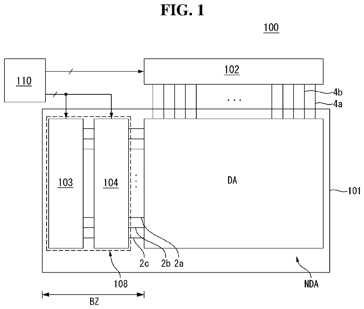
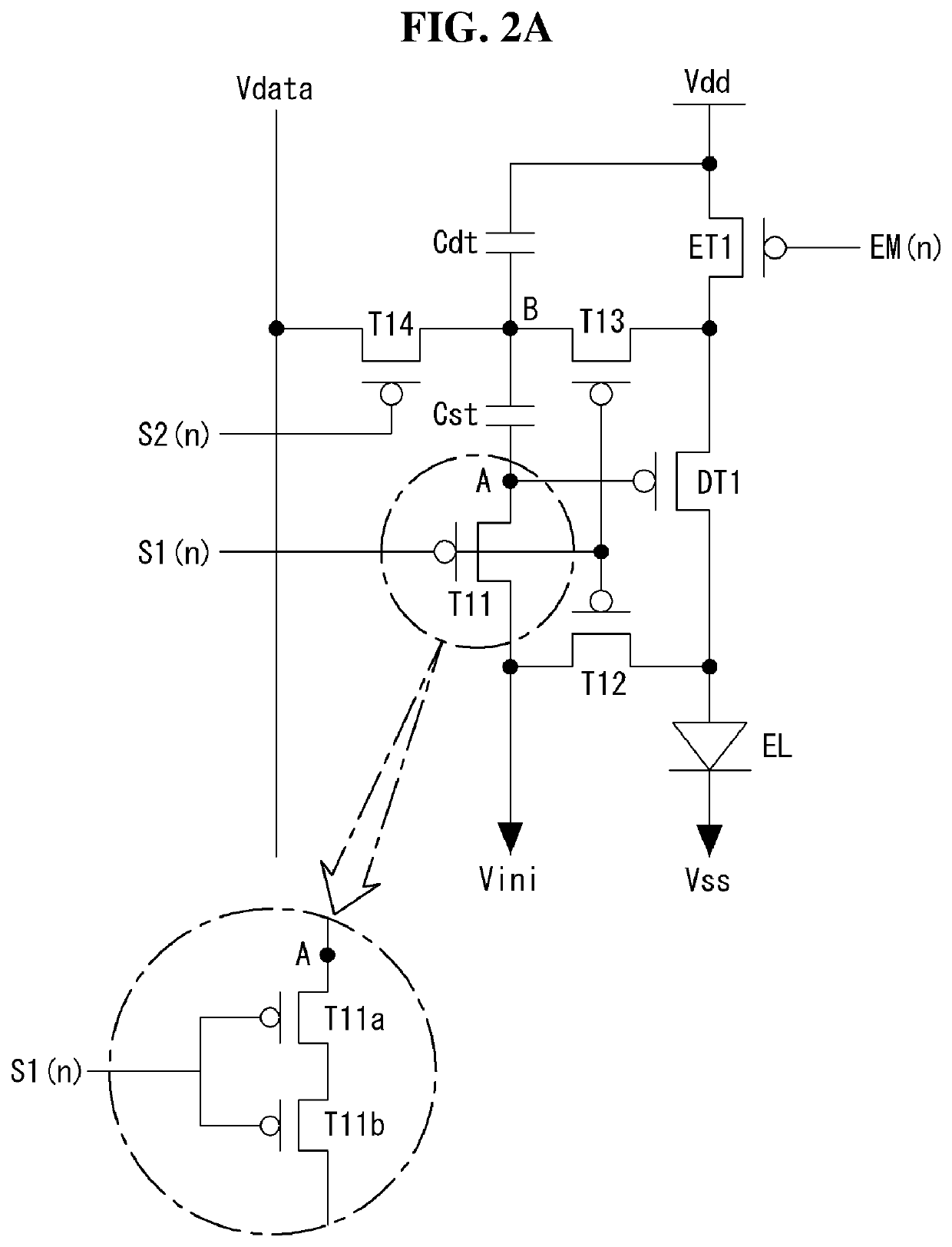
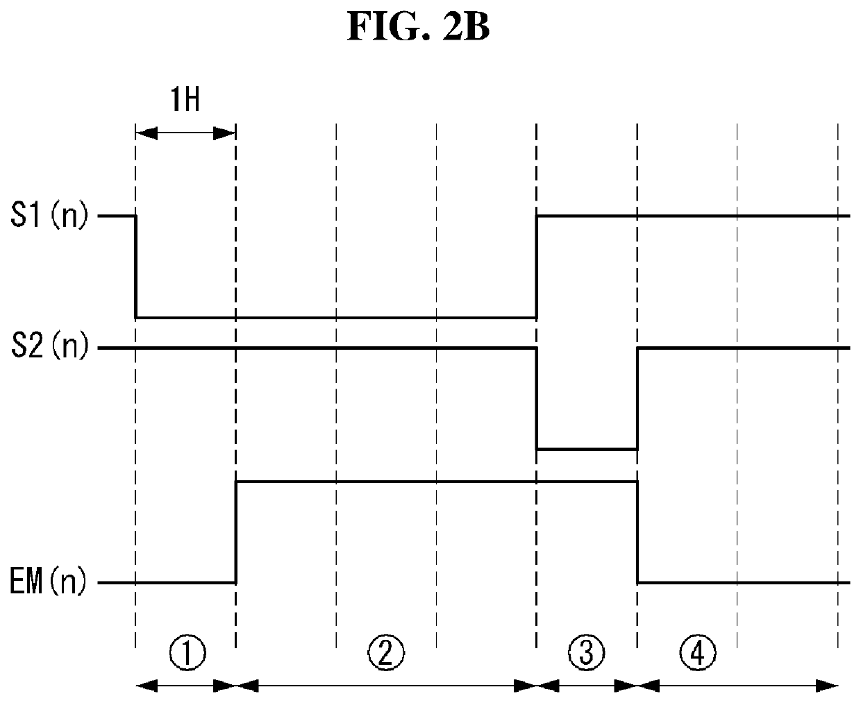
[0030]Advantages and features of the present disclosure, and implementation methods thereof will be clarified through the following aspects described with reference to the accompanying drawings. However, the present disclosure is not limited to aspects disclosed herein and may be implemented in various different forms. The aspects are provided for making the disclosure of the present disclosure thorough and for fully conveying the scope of the present disclosure to those skilled in the art. It is to be noted that the scope of the present disclosure is defined by the claims.

[0031]The figures, dimensions, ratios, angles, numbers, and the like disclosed in the drawings for describing the aspects of the present disclosure are merely illustrative and are not limited to matters shown in the present disclosure. Like reference numerals refer to like elements throughout. Further, in describing the present disclosure, detailed descriptions of well-known technologies will be omitted when it is...


PUM

PropertyMeasurementUnit
DAaaaaaaaaaa
potential voltageaaaaaaaaaa
voltageaaaaaaaaaa

Abstract

An electroluminescent display panel including a pixel driving circuit that includes a light-emitting element, a first capacitor connected to a first node and a second node, a second capacitor connected to the second node and a high potential voltage line, a driving transistor supplying electric current to the light-emitting element, a first switching circuit controlled by a first scan signal and turned on during the sampling period to compensate for a time-varying characteristic of the driving transistor, a second switching circuit controlled by a second scan signal and turned on during the programming period to apply a data voltage to the second node, and a light emission control circuit controlled by an emission signal and turned on during the initialization period and the emission period to apply the high potential voltage to the driving transistor.

Description

CROSS REFERENCE TO RELATED APPLICATION[0001]This application claims priority to and the benefit of Korean Patent Application No. 10-2019-0144624, filed on Nov. 12, 2019, which is hereby incorporated by reference in its entirety.BACKGROUNDField of the Disclosure[0002]The present disclosure relates to an electroluminescent display panel including a pixel driving circuit, and more particularly, to an electroluminescent display panel capable of high-resolution and high-frequency driving.Description of the Background[0003]With the development of information technology, the market for display devices, which are connection media between information and users, is growing. Beyond text-based information transfer, various types of communication are actively performed between users. As the type of information changes, the performance of a display device for displaying information is also developing. Accordingly, the use of various types of display devices such as an electroluminescent display, ...

Claims


Application Information

Patent Timeline
Patent Type & Authority Patents(United States)
IPC IPC(8): G09G3/325G09G3/3266G09G3/3291H01L27/32
CPCG09G3/325G09G3/3266G09G3/3291H01L27/3276G09G2310/0278G09G3/3208G09G3/3233G09G2300/0819G09G2300/0852G09G2300/0861G09G2320/0214G09G2300/0426G09G3/3275G09G2320/0233G09G2320/043G09G3/32G09G2320/0209G09G2320/0252G09G2320/0257G09G2300/0439G09G2340/04H10K59/131
Inventor KIM, JUNG CHUL
Owner LG DISPLAY CO LTD
Why Eureka
Try Eureka