Touch screen and display device

a display device and touch screen technology, applied in the field of display technologies, can solve problems such as prone to breakage of metal wiring, and achieve the effect of increasing the durability of bending of the touch screen

Inactive Publication Date: 2021-11-18
WUHAN CHINA STAR OPTOELECTRONICS SEMICON DISPLAY TECH CO LTD
View PDF5 Cites 2 Cited by
  • Summary
  • Abstract
  • Description
  • Claims
  • Application Information

AI Technical Summary

Benefits of technology

[0039]Compared with the conventional touch screen and display device, by electrically connecting the source and drain layer to the anode layer and electrically connecting the anode layer to the touch electrode layer, the touch screen and the display device of the present disclosure not only achieve the electrical connection between the layer and the touch electrode layer, but also increase durability of bending of the touch screen.

Problems solved by technology

Therefore, the metal wiring is prone to breakage.

Method used


Image

  • Touch screen and display device
  • Touch screen and display device
  • Touch screen and display device

Examples


Embodiment Construction

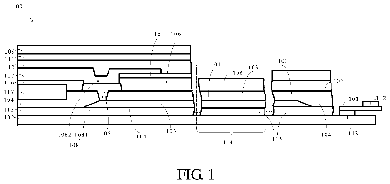
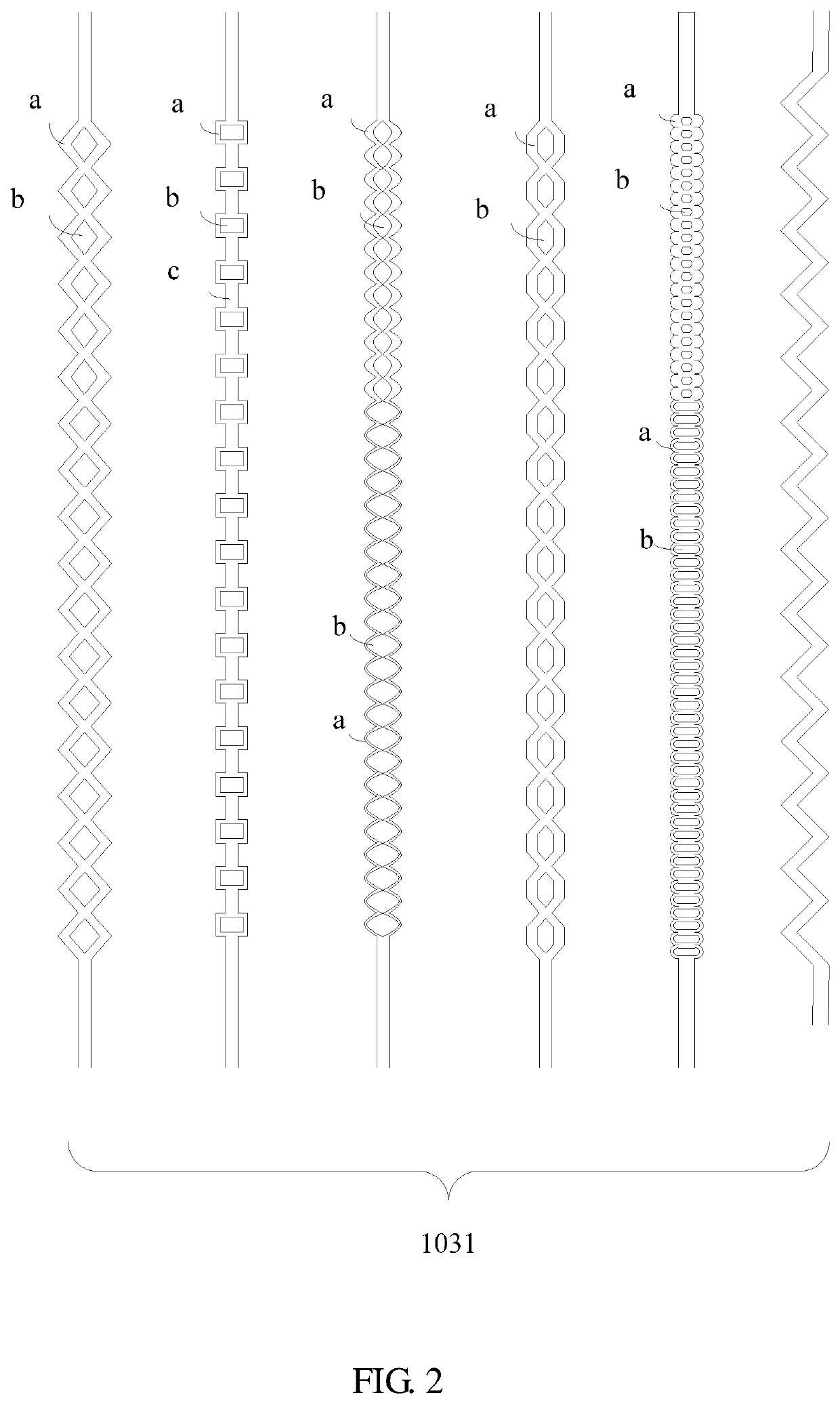
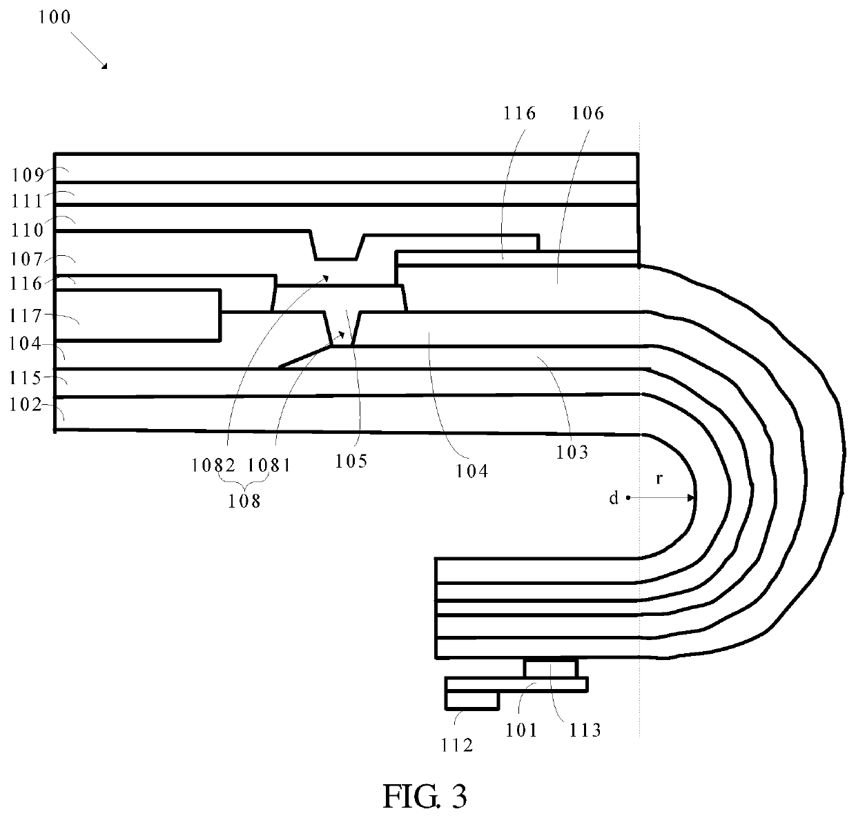
[0045]In the following detailed description, reference is made to the accompanying figures, in which various examples are shown by way of illustration. In this regard, directional terminology mentioned in the present disclosure, such as “top”, “bottom”, “front”, “back”, “left”, “right”, “inner”, “outer”, “lateral”, etc., is used with reference to the orientation of the figures being described. Therefore, the directional terminology is used for purposes of illustration and is not intended to limit the present invention.

[0046]In the accompanying figures, units with similar structures are indicated by the same reference numbers.

[0047]The term “embodiment” referred to herein means that a particular feature, structure, or property described in conjunction with the implementation may be contained in at least one implementation of the present disclosure. The phrase appearing in various places in the specification does not necessarily refer to the same implementation, nor does it refer to a...


PUM

PropertyMeasurementUnit
bending radiusaaaaaaaaaa

Abstract

A touch screen and a display device are provided. The touch screen includes a substrate, source and drain layers, a planarization layer, an anode layer, a pixel defining layer, and a touch electrode layer stacked in sequence. The touch screen further includes via holes, and the via hole includes a first via hole and a second via hole. The first via hole is defined on the planarization layer, the anode layer is electrically connected to the source and drain layer through the first via hole. The second via hole is defined on the pixel defining layer, and the touch electrode layer is connected to the anode layer through the second via hole.

Description

FIELD OF INVENTION[0001]The present disclosure relates to a field of display technologies, and more particular, to a touch screen and a display device.BACKGROUND OF INVENTION[0002]Current mainstream touch technologies include monolithic glass touch technology and in-cell touch technology. Touch screens are manufactured on display screens by the in-cell touch technology.[0003]The in-cell touch integrates a sensing circuit substrate with a display panel and is divided into on-cell technology and in-cell technology depending on different positions of the sensing circuit. Among those technology, the on-cell technology is widely used in organic light-emitting diode (OLED) display devices.[0004]In an OLED display device employing the on-cell technology, a touch electrode is disposed on a thin film encapsulation layer, one end of a metal wiring is connected to a touch electrode, and the other end of the metal wiring is connected to an array substrate. Because an organic light-emitting laye...

Claims


Application Information

Patent Timeline
Patent Type & Authority Applications(United States)
IPC IPC(8): G06F3/041H01L27/32H01L51/00H01L51/52
CPCG06F3/0412H01L27/323H01L27/3246H01L2251/5338H01L51/0097H01L51/5281G06F2203/04102H01L27/3276Y02E10/549G06F3/04164H10K59/40H10K59/131H10K50/86H10K2102/311H10K59/122H10K77/111
Inventor YE, JIAN
Owner WUHAN CHINA STAR OPTOELECTRONICS SEMICON DISPLAY TECH CO LTD
Why Eureka
Try Eureka