

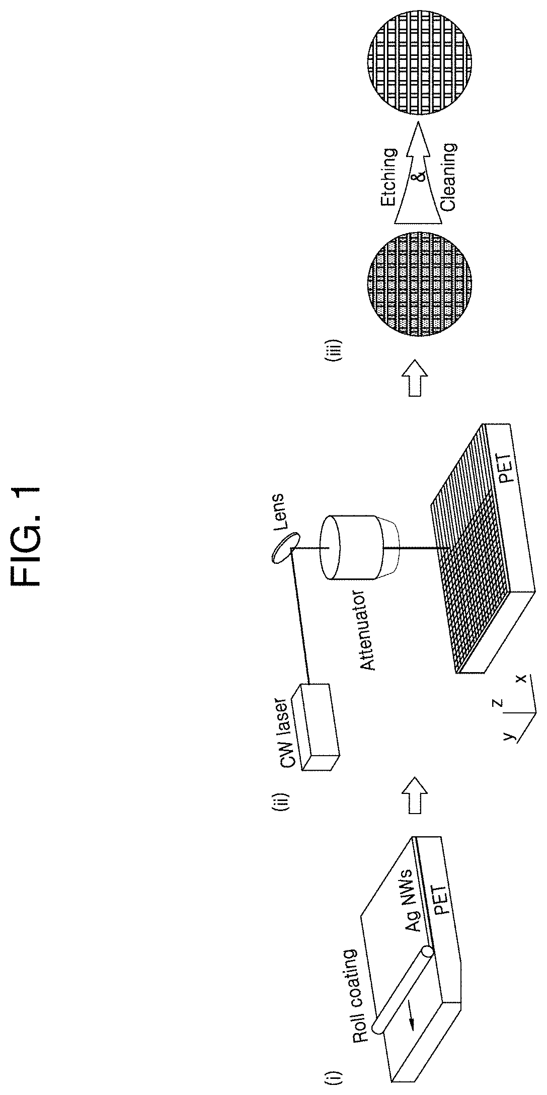
Silver nanowire-mesh (ag nw-mesh) electrode and manufacturing method thereof
a silver nanowire and mesh technology, applied in the direction of conductive layers on insulating supports, nuclear elements, conductive material removal by irradiation, etc., can solve the problems of conductive polymers and carbon-based transparent electrodes that are still less than, fragile ito electrodes, and unsuitable for flexible devices. , to achieve the effect of high bending durability
- Summary
- Abstract
- Description
- Claims
- Application Information
AI Technical Summary
Benefits of technology
Problems solved by technology
Method used
Image

Examples
example 1
[0056]FIG. 4A to FIG. 4D show SEM images and atomic force microscopy 3-dimensional (AFM 3D) images of the nanowire network structure before and after laser fusion. As shown in FIG. 4A, in a pristine Ag NWs network before laser fusion, the Ag NWs were simply stacked and electrically weakly connected, which led to the increase in contact resistance and degradation of electrical characteristics. In addition, the mechanical characteristics were low due to a weak adhesion between the pristine Ag NWs network and the PET substrate. On the other hand, FIG. 4B shows a Ag NWs electrode in which nanowires were completely bonded by laser welding to form a network structure. Therefore, the electrical connection path of Ag NWs increased, and strong adhesion to the substrate was observed. FIG. 4C and FIG. 4D show surface 3D images and roughness of each Ag NWs. As shown in FIG. 4C and FIG. 4D, the roughness of Ag NWs before selective laser welding was 31.6 nm, and after laser welding, the roughness...
example 2
[0058]FIG. 5A to FIG. 5C present graphs showing changes in line width according to laser power and laser scan speed during SLW. Laser welding conditions varied according to the amount of pristine Ag NWs deposited on the substrate through a solution process before laser welding was performed. For a quantitative analysis of the number of nanowires forming a random network on the substrate, a description is made through area mass density (AMD). As AMD increases, the number of nanowires of a random network deposited on the substrate increases, which means that heat can be absorbed well, and accordingly, an Ag NW-mesh may be produced even at lower laser power and faster laser scan speed. That is, as the AMD increases, the usable range of laser conditions used to manufacture Ag NW-mesh is widened.
[0059]FIG. 5A to FIG. 5C are 3D graphs showing laser power and laser scan speed conditions of SLW for producing an Ag NW-mesh when the AMD of the Ag NWs increases to 88.5 mg / m2, 104.5 mg / m2, and ...
example 3
[0060]FIG. 6A to FIG. 6I show SEM images when the energy density calculated from laser scan speed and laser power is changed to 3 J / cm2 (FIG. 6A to FIG. 6C), 2 J / cm2 (FIG. 6D to FIG. 6F, and 1 J / cm2 (FIG. 6G to FIG. 6I) and AMD increases to 88.5 mg / m2 (FIG. 6A, FIG. 6D, and FIG. 6G), 104.5 mg / m2 (FIG. 6B, FIG. 6E, and FIG. 6H), and 126.2 mg / m2 (FIG. 6C, FIG. 6F, and FIG. 6I). As shown in FIG. 6C and FIG. 6F, the Ag NW-mesh was over-welded by excessive heat being applied due to high energy density attributed to the high laser power and the low laser scan speed. On the contrary, FIG. 6G shows an imcompletely welded Ag NW-mesh due to the low energy density attributed to the low laser power and the fast laser scan speed.
[0061]FIG. 7A to FIG. 7E and FIG. 8A to FIG. 8E show enlarged SEM images and AFM z-axis cross-sectional profile graphs of an Ag NW-mesh fabricated by reducing the laser density by gradually increasing a laser scan speed to 0.3 m / s, 0.5 m / s, 0.7 m / s, 1 m / s, and 1.5 m / s wi...
PUM
| Property | Measurement | Unit |
|---|---|---|
| angle | aaaaa | aaaaa |
| angle | aaaaa | aaaaa |
| angle | aaaaa | aaaaa |
Abstract
Description
Claims
Application Information