Thin-film transistor having oxide semiconductor channel layer vertically exending along lateral sides of source electrode, separation layer, and drain electrode and array substrate including same

a thin-film transistor and semiconductor channel technology, applied in the field of thin-film transistors, can solve the problems of the size of a thin-film transistor, and achieve the effects of improving the electrical performance improving the bending durability of the thin-film transistor, and reducing the area of a pixel

Active Publication Date: 2019-11-19
WUHAN CHINA STAR OPTOELECTRONICS SEMICON DISPLAY TECH CO LTD
View PDF10 Cites 1 Cited by
  • Summary
  • Abstract
  • Description
  • Claims
  • Application Information

AI Technical Summary

Benefits of technology

[0006]An objective of the present invention are to provide a thin-film transistor, which allows for significant reduction of the size of the thin-film transistor and helps reduce a pixel area, and is particularly fit to a high-definition flexible display.
[0007]Another objective of the present invention is to provide a thin-film transistor fabrication method, which significantly reduces of the size of a thin-film transistor, helps reduce a pixel area, and is less complicated in a fabrication process thereof.
[0042]The efficacy of the present invention is that the present invention provides a the thin-film transistor, which is structured such that a separation layer is arranged between a source electrode and a drain electrode and an oxide semiconductor channel layer is arranged on one side of the separation layer and the drain electrode and sequentially contacts a portion of the upper surface of the drain electrode, a side surface of the drain electrode and the organic separation layer, and a portion of the upper surface of the source electrode to provide a vertical channel, wherein a channel length corresponds to a thickness of the separation layer, so that varying the thickness of the separation layer may reduce the length of the vertical channel to a sub-micrometer order to thereby significantly reduce the size of the thin-film transistor. Since the vertical channel has a relatively small overlapping area with a scan line and a data line, the area of a pixel can be reduced. The vertical channel does not cause short channel effect, allowing for improvement of the electrical performance of the thin-film transistor. Using a multiple-layered hexagonal boron nitride film to make a moisture / oxygen barrier layer and using a double-layered graphene film to make the source electrode and the drain electrode, bending durability of the thin-film transistor can be improved. The present invention provides a thin-film transistor fabrication method, which is implemented to make the above vertical-channel thin-film transistor, so as to significantly reduce the size of the thin-film transistor, reduce an area of a pixel, improve electrical characteristics and bending durability of the thin-film transistor. In addition, one single mask is used to simultaneously form the oxide semiconductor channel layer, the gate insulation layer, and the gate electrode, so that complication of the fabrication process is reduced. The present invention provides an array substrate, which comprises a plurality of above-described vertical-channel thin-film transistors arranged in an array and has a relatively small size, making an area of a pixel relatively small.

Problems solved by technology

Particularly, for high definition flexible mobile phone display screens, virtual reality (VR) display screens, augmented reality (AR) display screens, and holographic display screens that are still under development, the most concerned issue is to reduce the area of a pixel and the size of a thin-film transistor.

Method used


Image

  • Thin-film transistor having oxide semiconductor channel layer vertically exending along lateral sides of source electrode, separation layer, and drain electrode and array substrate including same
  • Thin-film transistor having oxide semiconductor channel layer vertically exending along lateral sides of source electrode, separation layer, and drain electrode and array substrate including same
  • Thin-film transistor having oxide semiconductor channel layer vertically exending along lateral sides of source electrode, separation layer, and drain electrode and array substrate including same

Examples


Embodiment Construction

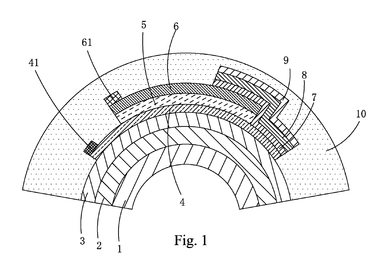
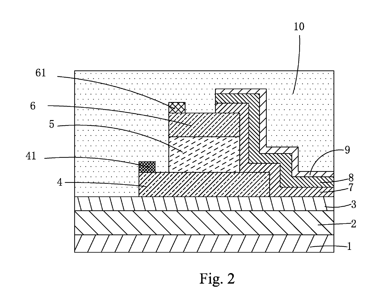
[0055]To further expound the technical solution adopted in the present invention and the advantages thereof, a detailed description will be given with reference to the preferred embodiments of the present invention and the drawings thereof.

[0056]Referring to both FIGS. 1 and 2, firstly, the present invention provides a thin-film transistor, which comprises:

[0057]a flexible backing 1;

[0058]a moisture / oxygen barrier layer 2 arranged on the flexible backing 1;

[0059]a buffer layer 3 arranged on the moisture / oxygen barrier layer 2;

[0060]a source electrode 4 arranged on the buffer layer 3;

[0061]a separation layer 5 arranged on the source electrode 4 and exposing at least one side portion of the source electrode 4;

[0062]a drain electrode 6 arranged on the separation layer 5;

[0063]an oxide semiconductor channel layer 7 arranged at one side of the separation layer 5 and the drain electrode 6 to sequentially contact a portion of an upper surface of the drain electrode 6, a side surface of the...


PUM


Abstract

The present invention provides a thin-film transistor and a fabrication method thereof, and an array substrate. The thin-film transistor includes a separation layer (5) arranged between the source electrode (4) and the drain electrode (6). An oxide semiconductor channel layer (7) is arranged on one side of the separation layer (5) and the drain electrode (6) to contact a portion of an upper surface of the drain electrode (6), a side surface of the drain electrode (6) and the organic separation layer (5), and a portion of an upper surface of the source electrode (4) to serve as a vertical channel, of which a channel length corresponds to a thickness of the separation layer (5). Varying the thickness of the separation layer to reduce the length of the vertical channel to a sub-micrometer order would greatly reduce the size of the thin-film transistor and reduce the area of a pixel. The vertical channel does not cause a short channel effect so as to improve electrical performance of the thin-film transistor. Using a multiple-layered hexagonal boron nitride film to make a moisture / oxygen barrier layer (2) and using a double-layered graphene film to make the source electrode (4) and the drain electrode (6) help significantly improve bending durability of the thin-film transistor.

Description

BACKGROUND OF THE INVENTION1. Field of the Invention[0001]The present invention relates to the field of display technology, and more particular to a thin-film transistor and a fabrication method thereof and an array substrate.2. The Related Arts[0002]In the field of display technology, flat panel displays, such as liquid crystal displays (LCDs) and organic light-emitting diode (OLED) displays, have gradually taken the place of cathode ray tube (CRT) displays.[0003]At present, a mainstream LCD is generally made up of a thin-film transistor (TFT) array substrate and a color filter (CF) substrate that are laminated to each other; and liquid crystal is filled between the array substrate and the CF substrate. Electricity is applied to change the direction of liquid crystal molecules in order to refract out light from a backlight module to generate an image.[0004]OLED has various advantages, such as being self-luminous, low drive voltage, high light emission efficiency, short response tim...

Claims


Application Information

Patent Timeline
Patent Type & Authority Patents(United States)
IPC IPC(8): H01L29/66H01L29/786H01L29/45H01L21/443H01L27/12
CPCH01L29/7869H01L29/78603H01L29/45H01L29/78696H01L29/66969H01L29/78642H01L21/443H01L27/1218H01L27/1225H01L29/0646H01L29/41H01L29/66742H01L29/42384
Inventor BU, CHENGHAO
Owner WUHAN CHINA STAR OPTOELECTRONICS SEMICON DISPLAY TECH CO LTD
Why Eureka
Try Eureka