Display device

a technology of display device and display screen, which is applied in the direction of semiconductor devices, organic semiconductor devices, electrical devices, etc., to achieve the effect of reducing or minimizing the size of the light emission area

Pending Publication Date: 2022-06-30
LG DISPLAY CO LTD
View PDF0 Cites 0 Cited by
  • Summary
  • Abstract
  • Description
  • Claims
  • Application Information

AI Technical Summary

Benefits of technology

[0006]The present disclosure has been made in view of various technical problems including the above problems, and various embodiments of the present disclosure provide a display device that may reduce or minimize a size of a light emission area that becomes a dark spot.

Problems solved by technology

For this reason, the display device has a problem in that all of subpixels in which particles occur become dark spots so as not to emit light.

Method used


Image

  • Display device
  • Display device
  • Display device

Examples


Embodiment Construction

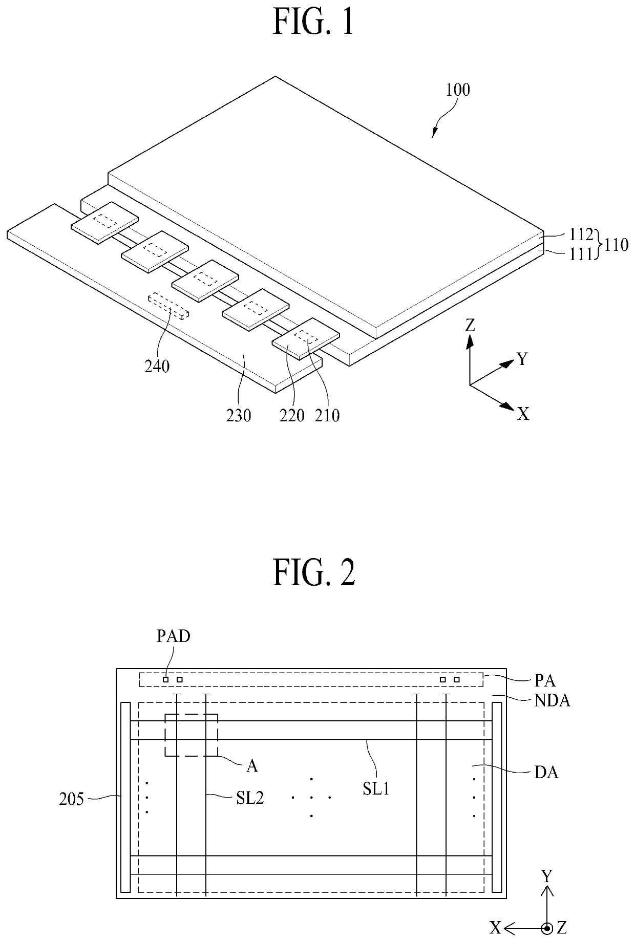
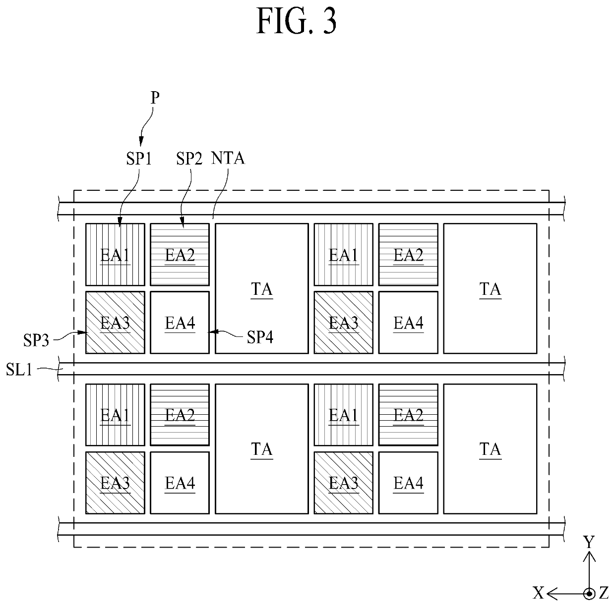
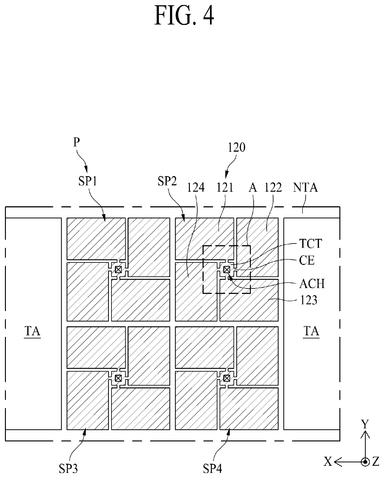
[0023]Advantages and features of the present disclosure, and implementation methods thereof will be clarified through following embodiments described with reference to the accompanying drawings. The present disclosure may, however, be embodied in different forms and should not be construed as limited to the embodiments set forth herein. Rather, these embodiments are provided so that this disclosure will be thorough and complete, and will fully convey the scope of the present disclosure to those skilled in the art.

[0024]A shape, a size, a ratio, an angle, and a number disclosed in the drawings for describing embodiments of the present disclosure are merely an example, and thus, the present disclosure is not limited to the illustrated details. Like reference numerals refer to like elements throughout the specification. In the following description, when the detailed description of the relevant known function or configuration is determined to unnecessarily obscure the technical feature...


PUM

PropertyMeasurementUnit
area DAaaaaaaaaaa
area DAaaaaaaaaaa
light transmittanceaaaaaaaaaa

Abstract

A display device may reduce or minimize a size of a light emission area that becomes a dark spot due to particles. The display device includes a substrate provided with a display area for displaying an image by subpixels, first electrodes provided in each of the subpixels over the substrate, driving transistors provided between the substrate and the first electrodes and coupled to each of the first electrodes, a light emitting layer provided over the first electrodes, and a second electrode provided over the light emitting layer. Each of the first electrodes includes divided electrodes spaced apart from each other, a transistor contact portion coupled with the driving transistor through a contact hole, and connection electrodes coupling each of the plurality of divided electrodes with the transistor contact portion.

Description

BACKGROUNDTechnical Field[0001]The present disclosure relates to a display device.Description of the Related Art[0002]A display device may include a first electrode, a light emitting layer, and a second electrode, which are sequentially deposited, and may emit light through the light emitting layer when a voltage is applied to the first electrode and the second electrode. In this display device, particles may occur on the first electrode during a manufacturing process, and in this case, a short may occur between the first electrode and the second electrode in the area where the particles occur. For this reason, the display device has a problem in that all of subpixels in which particles occur become dark spots so as not to emit light.[0003]Recently, studies for a transparent display device in which a user may view objects or images positioned at an opposite side by transmitting the display device are actively ongoing.[0004]The transparent display device includes a display area on wh...

Claims


Application Information

Patent Timeline
Patent Type & Authority Applications(United States)
IPC IPC(8): H01L27/32H01L51/52
CPCH01L27/3218H01L27/3246H01L2251/308H01L51/5234H01L27/3276H01L51/5218H10K59/123H10K59/12H10K59/131H10K50/805H10K59/121H10K50/813H10K50/818H10K2102/341H10K71/861H10K59/124H10K59/1213H10K59/122H10K59/353H10K50/828H10K2102/103
Inventor YOON, DOOHYUNEOM, HYESEONKIM, HYOUNG-SUKIM, MOONSOO
Owner LG DISPLAY CO LTD
Why Eureka
Try Eureka