Check patentability & draft patents in minutes with Patsnap Eureka AI!

Semiconductor memory device and memory system for improving bus efficiency

a memory device and semiconductor technology, applied in the direction of memory adressing/allocation/relocation, digital storage, instruments, etc., can solve the problems of reducing the bus efficiency of memory systems, reducing the overall performance of computer systems, and cpus operating speed gap

Inactive Publication Date: 2002-08-20
SAMSUNG ELECTRONICS CO LTD
View PDF3 Cites 21 Cited by
  • Summary
  • Abstract
  • Description
  • Claims
  • Application Information

AI Technical Summary

Benefits of technology

This solution enhances bus efficiency by allowing consecutive data reads from multiple memory modules without data-empty spaces on the data bus, thereby improving the overall performance of memory systems.

Problems solved by technology

As a result, there arises a gap between the operating speeds of CPUs and memory devices.
The slower operating speeds of memory devices restrict the overall performance of computer systems.
Hence, synchronous DRAMs degrade the bus efficiency of memory systems and consequently restrict the performance of memory systems.
Thus, the bus efficiency is degraded and the performance of the memory system is restricted.
According to the conventional memory design and protocol, the column address lines are shared with the row address and application of concurrent CA1 and RA2 addresses will result in an erroneous read operation.

Method used


Image

  • Semiconductor memory device and memory system for improving bus efficiency
  • Semiconductor memory device and memory system for improving bus efficiency
  • Semiconductor memory device and memory system for improving bus efficiency

Examples


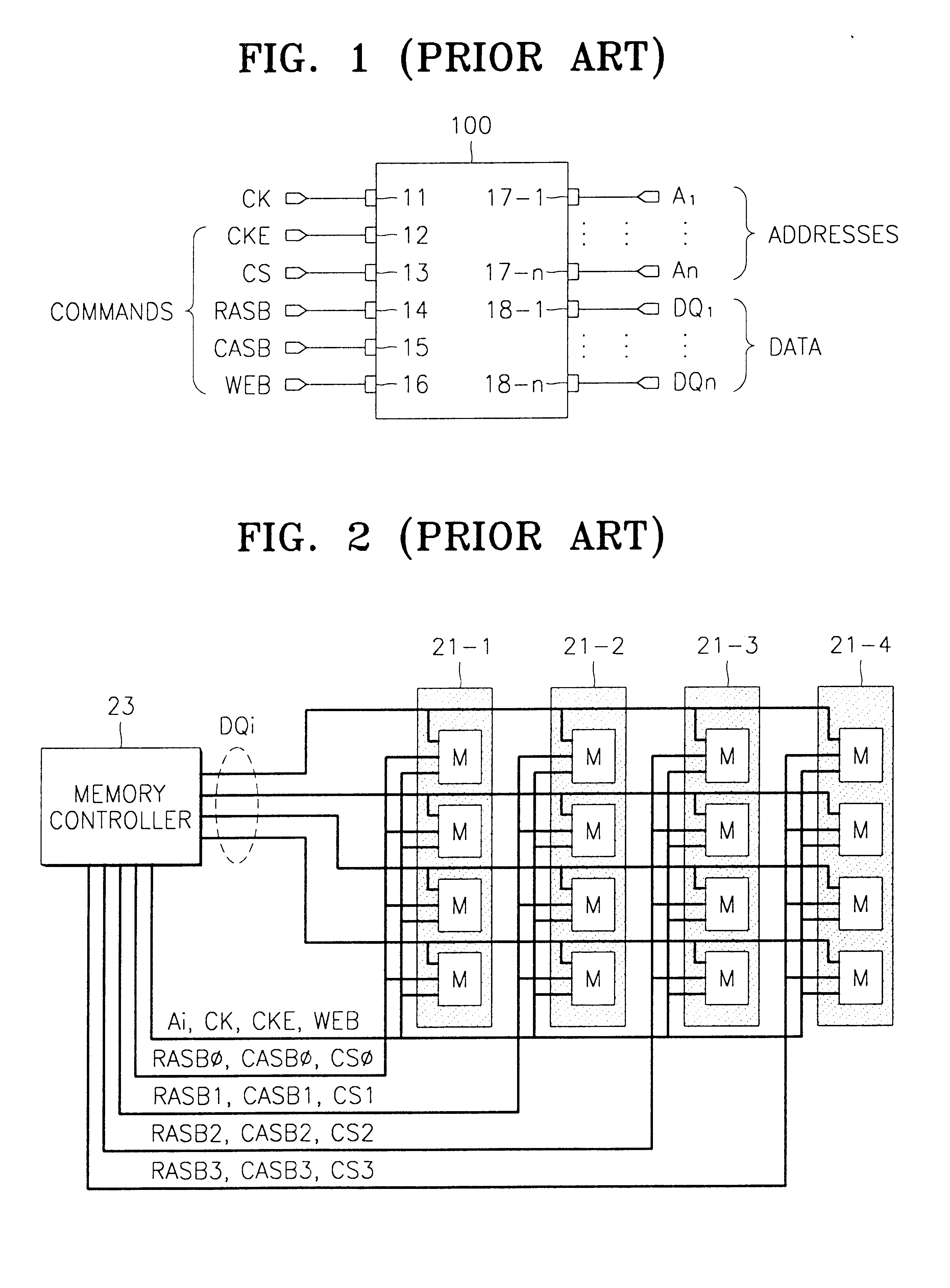
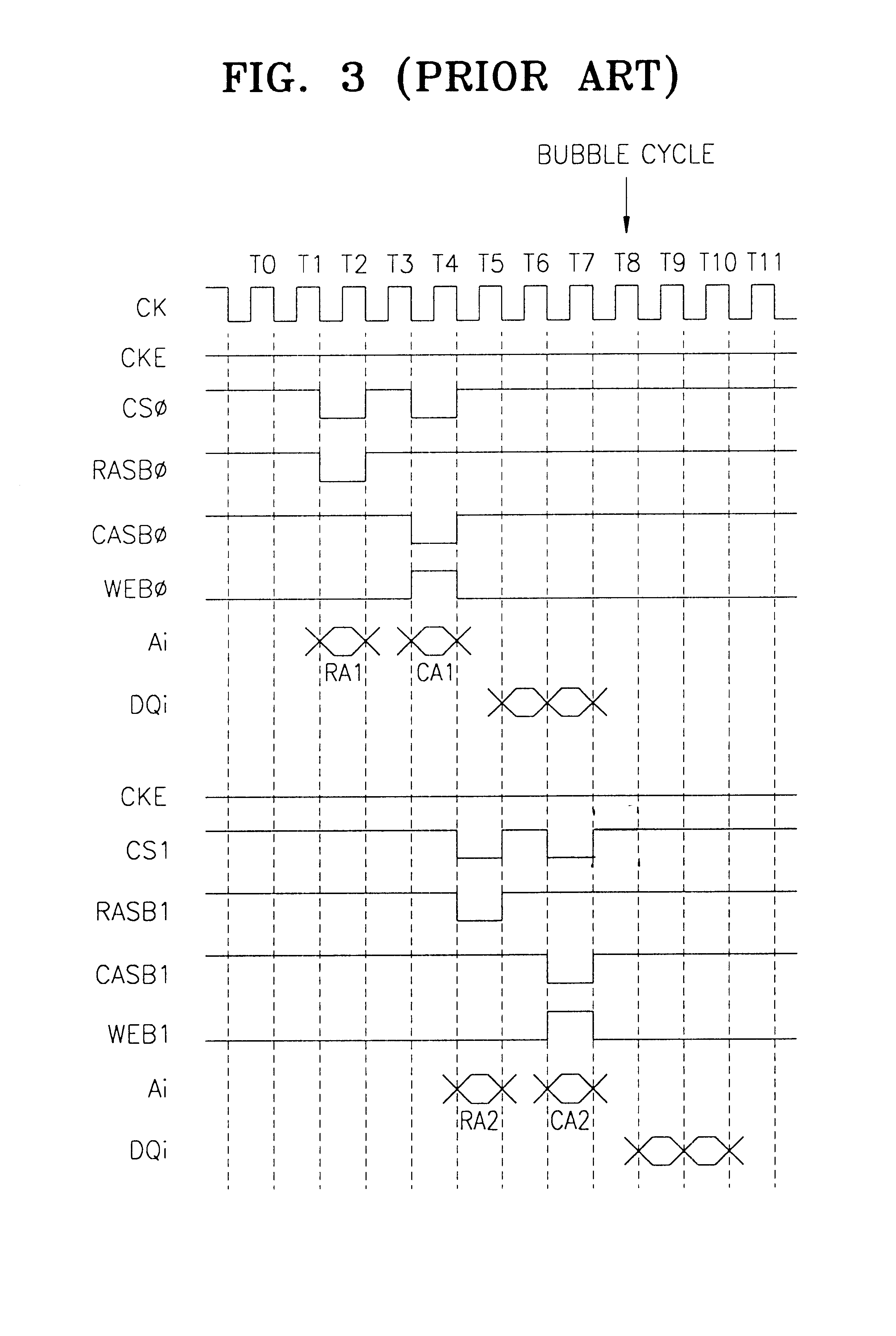
Embodiment Construction

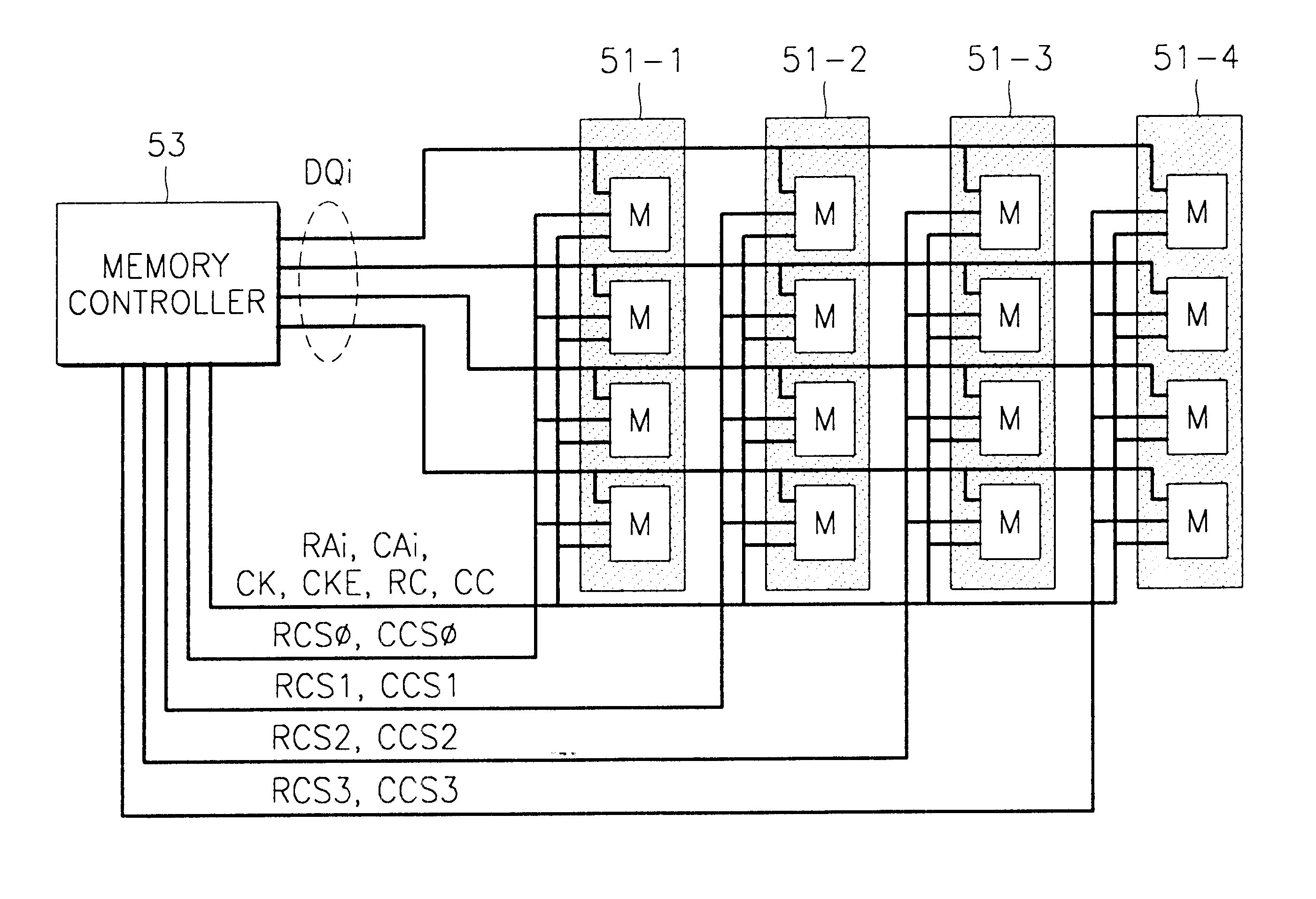
Referring to FIG. 4, a semiconductor memory device 400 according to the present invention is a dynamic random access memory (DRAM) having an illustrative pin configuration which includes a first chip selection signal input pin 43 for receiving a first chip selection signal RCS for a row address strobe from a memory controller, and a separate second chip selection signal input pin 44 for receiving a second chip selection signal CCS for a column address strobe from a memory controller. The figure shows only pins associated with data input and the actual arrangement shown is not critical to the invention.

According to a preferred embodiment of the present invention, the semiconductor memory device 400 also separately includes a row command input pin 45 for receiving a row command RC from a memory controller, and a column command input pin 46 for receiving a column address strobe CC from a memory controller.

The semiconductor memory device 400 also separately includes a plurality of row a...


PUM


Abstract

Disclosed is a memory device, comprising a memory controller, a clock input pin for receiving a clock signal, a first chip selection signal input pin for receiving a first chip selection signal for a row address strobe from the memory controller, a second chip selection signal input pin for receiving a second chip selection signal for a column address strobe from the memory controller, a row command input pin for receiving a row command from the memory controller, a column command input pin for receiving a column command from the memory controller, a plurality of row address input pins for receiving row addresses from the memory controller, and a plurality of column address input pins for receiving column addresses from the memory controller.

Description

1. Field of the InventionThe present invention relates to a semiconductor memory device and a memory system, and more particularly, to a semiconductor memory device and a memory system for improving bus efficiency.2. Description of the Related ArtMemory devices are typically developed to have a high density of integration and large capacity. Central processing units (CPU) are developed to achieve processing at high speed. The operating speed of large memory devices is usually slower than the speed of the CPUs. As a result, there arises a gap between the operating speeds of CPUs and memory devices. The slower operating speeds of memory devices restrict the overall performance of computer systems. In order to achieve speedy memory systems, high-speed memory devices must be developed and the bus efficiency thereof improved.Synchronous DRAMs are among the fastest large-scale memory devices. However, in synchronous DRAMs, in order to reduce the number of pins, a row command (RAS) and a c...

Claims


Application Information

Patent Timeline
Patent Type & Authority Patents(United States)
IPC IPC(8): G11C11/4096G11C7/00G11C7/10G11C7/22G11C8/18G11C8/00G11C11/409G06F12/02G11C11/407G11C11/401G11C11/4063
CPCG11C7/1006G11C7/1072G11C7/22G11C8/18G11C11/4096G11C11/4063
Inventor KYUNG, KYE-HYUN
Owner SAMSUNG ELECTRONICS CO LTD
Features
  • R&D
  • Intellectual Property
  • Life Sciences
  • Materials
  • Tech Scout
  • Unparalleled Data Quality
  • Higher Quality Content
  • 60% Fewer Hallucinations
Learn More