Method of forming a color filter layer on an array substrate and device thereof

Inactive Publication Date: 2005-08-23
INNOLUX CORP
View PDF8 Cites 5 Cited by
  • Summary
  • Abstract
  • Description
  • Claims
  • Application Information

AI Technical Summary

Benefits of technology

[0006]One aspect of the present invention provides a color liquid crystal display device. The color liquid crystal display device includes an array substrate, a black matrix layer, a black matrix frame around the periphery of the black matrix layer, and a color filter layer. The feature of the device is that the color filter layer extends to cover the black matrix frame, so the difference in thickness of the liquid crystal regions over the color filter layer and over the black matrix frame is decreased. The red, green and blue color filters covering the black matrix frame may be an additional dielectric layer abating the circuit loading, and the thickness of the color filter layer is flexible. Accordingly, the circuit loading can meet standards and the device can perform normally without altering the cell gap. In the mean time, the above-mentioned drawbacks are overcome, and the producing process is simplified. The array substrate includes a scan line and a data line forming a pixel, on which a thin film transistor is formed; a pixel electrode is connected to the thin film transistor. The color filter layer includes red, green and blue filters, and is formed on the array substrate and the black matrix layer.
[00

Problems solved by technology

Some heating steps, e.g. pre-baking, exposure or post-exposure baking, during the process of forming the upper substrate may lead to deformation of the upper substrate, so that misalignment of the upper and lower substrates may happen during assembly.
However, increasing the thi

Method used


Image

  • Method of forming a color filter layer on an array substrate and device thereof
  • Method of forming a color filter layer on an array substrate and device thereof
  • Method of forming a color filter layer on an array substrate and device thereof

Examples


Example

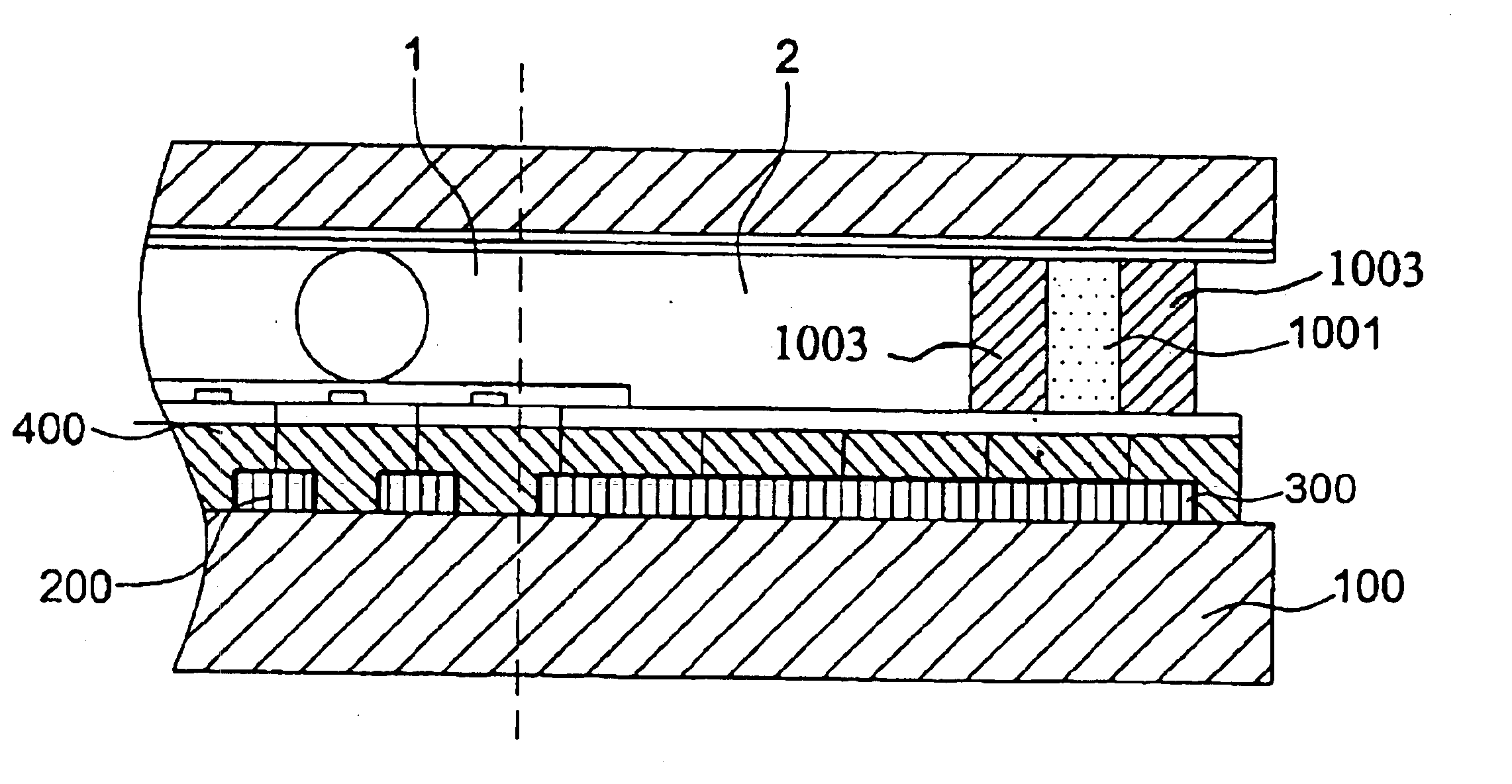
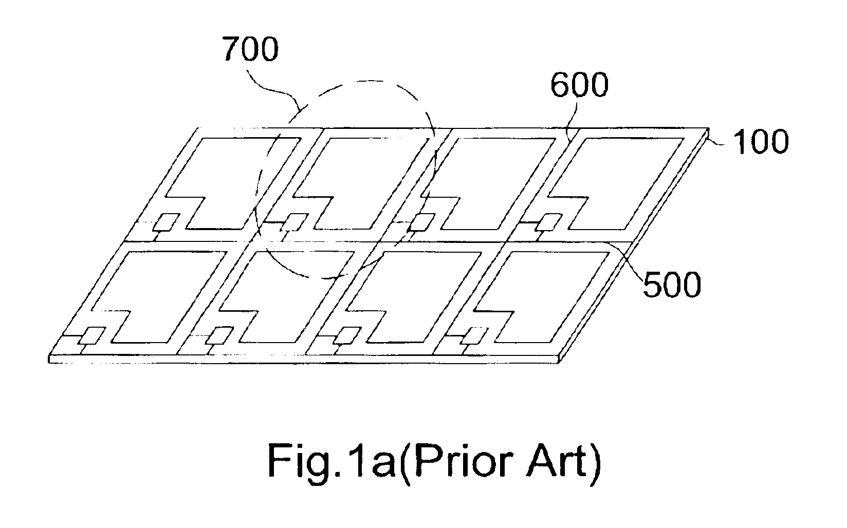
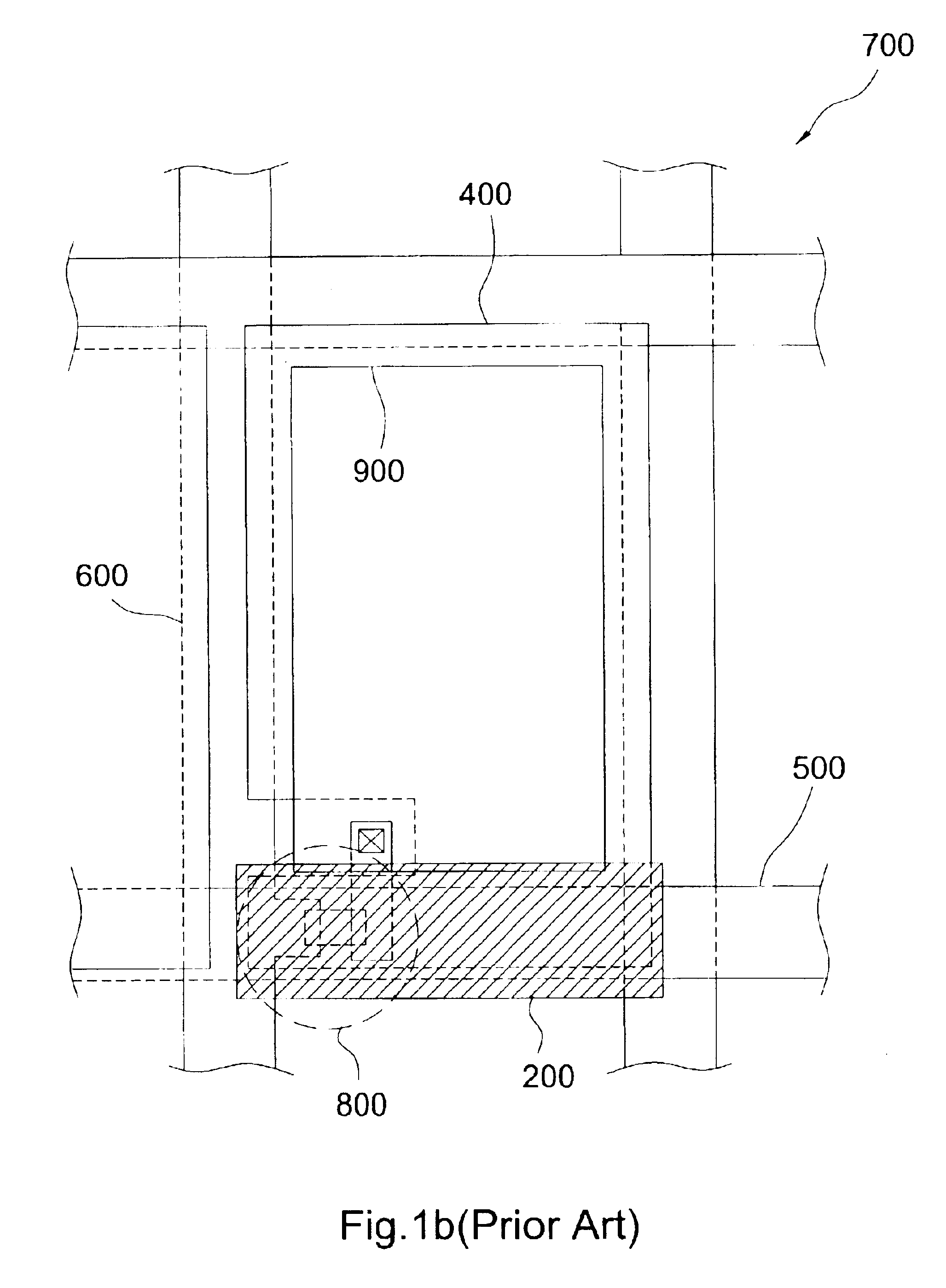
[0013]A color liquid crystal display device is provided as shown in FIG. 4. The device includes an array substrate 100 and a black matrix layer 200 formed on the array substrate 100. A black matrix frame 300 is formed around the periphery of the black matrix layer 200 to prevent light leakage from the backlight. A color filter layer 400 is formed on the array substrate 100 and the black matrix layer 200. The feature of the device is that the color filter layer 400 extends to cover the black matrix frame 300, so the difference in thickness between the liquid crystal region 1 and the liquid crystal region 2 is decreased. The red, green and blue color filters covering the black matrix frame 300 may be an additional dielectric layer abating the circuit loading, and the thickness of the color filter layer 400 is flexible. Accordingly, the circuit loading can meet standards and the device can perform normally without altering the cell gap. In the meantime, the above-mentioned drawbacks ar...


PUM


Abstract

The present invention provides a color liquid crystal display device in which a color filter layer is formed on an array substrate. The array substrate includes a scan line and a data line forming a pixel, on which a thin film transistor is formed, and a pixel electrode is connected to the thin film transistor. A black matrix layer is formed on the array substrate. A black matrix frame is formed around the periphery of the black matrix layer. A color filter layer is formed on the array substrate and the black matrix layer, and extends to cover the black matrix frame.

Description

FIELD OF INVENTION[0001]The present invention relates to a color liquid crystal display device in which a color filter layer and a black matrix layer are formed on an array substrate.BACKGROUND OF THE INVENTION[0002]A typical liquid crystal display device includes an upper substrate, a lower substrate, and a liquid crystal layer between them. The upper substrate has a color filter layer and a common electrode. The lower substrate, referred to as an array substrate, has a switching unit and a pixel electrode. The upper and lower substrates are individually fabricated and then assembled together. Some heating steps, e.g. pre-baking, exposure or post-exposure baking, during the process of forming the upper substrate may lead to deformation of the upper substrate, so that misalignment of the upper and lower substrates may happen during assembly. However, this problem may be solved and the producing process may be simplified by putting a color filter layer and a black matrix layer on the...

Claims


Application Information

Patent Timeline
IPC IPC(8): G02F1/1335G02F1/13G02F1/1333
CPCG02F1/133512G02F1/133514G02F2001/133388G02F1/133388
Inventor PENG, HUO-LONGCHIU, CHAUNG-MINGKUO, KUANG-LUNGCHANG, JING-YIYANG, TZU-SENG
Owner INNOLUX CORP
Why Eureka
Try Eureka