
Method of processing a substrate
- Summary
- Abstract
- Description
- Claims
- Application Information
AI Technical Summary
Benefits of technology
Problems solved by technology
Method used
Image

Examples
Embodiment Construction
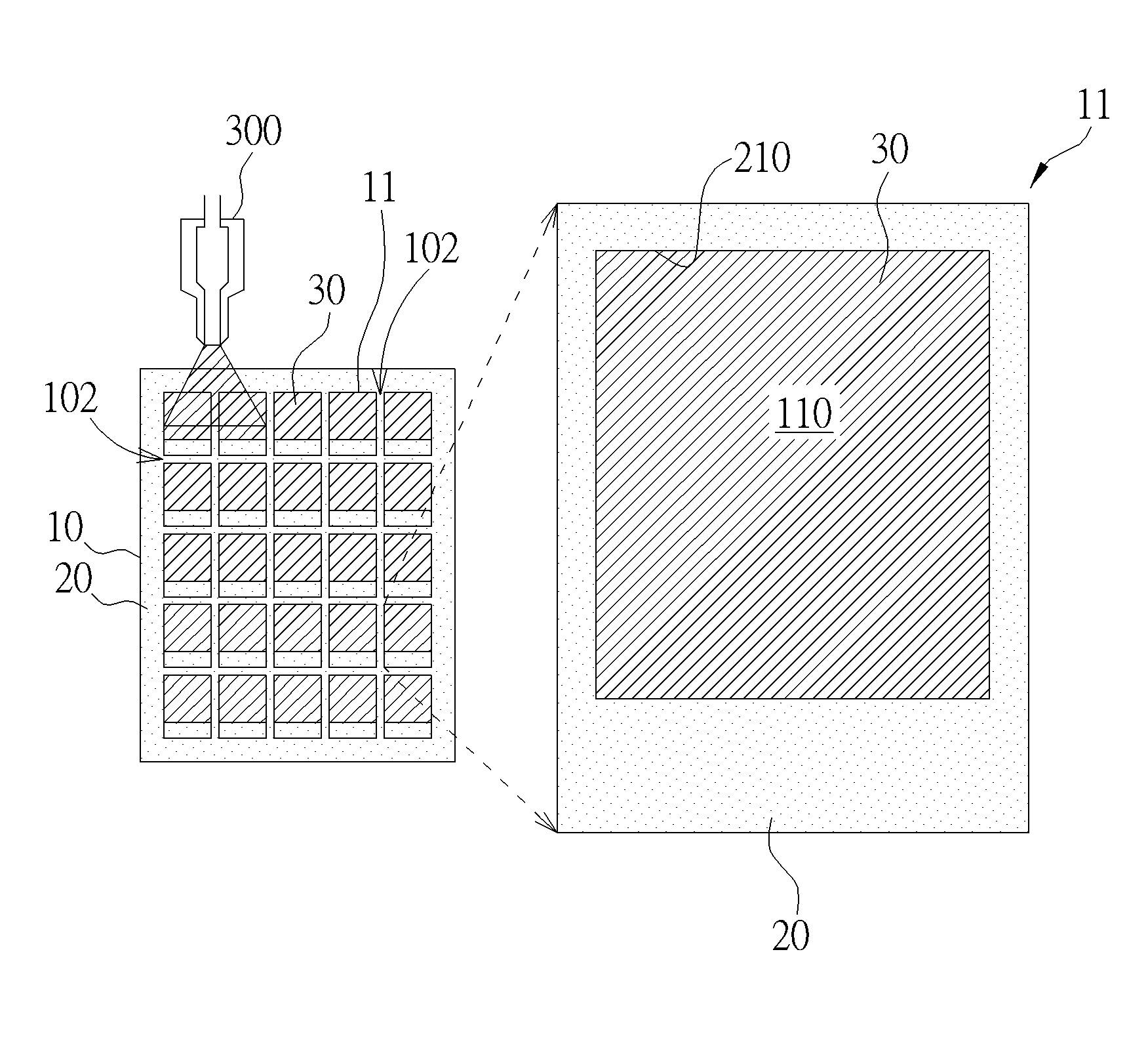
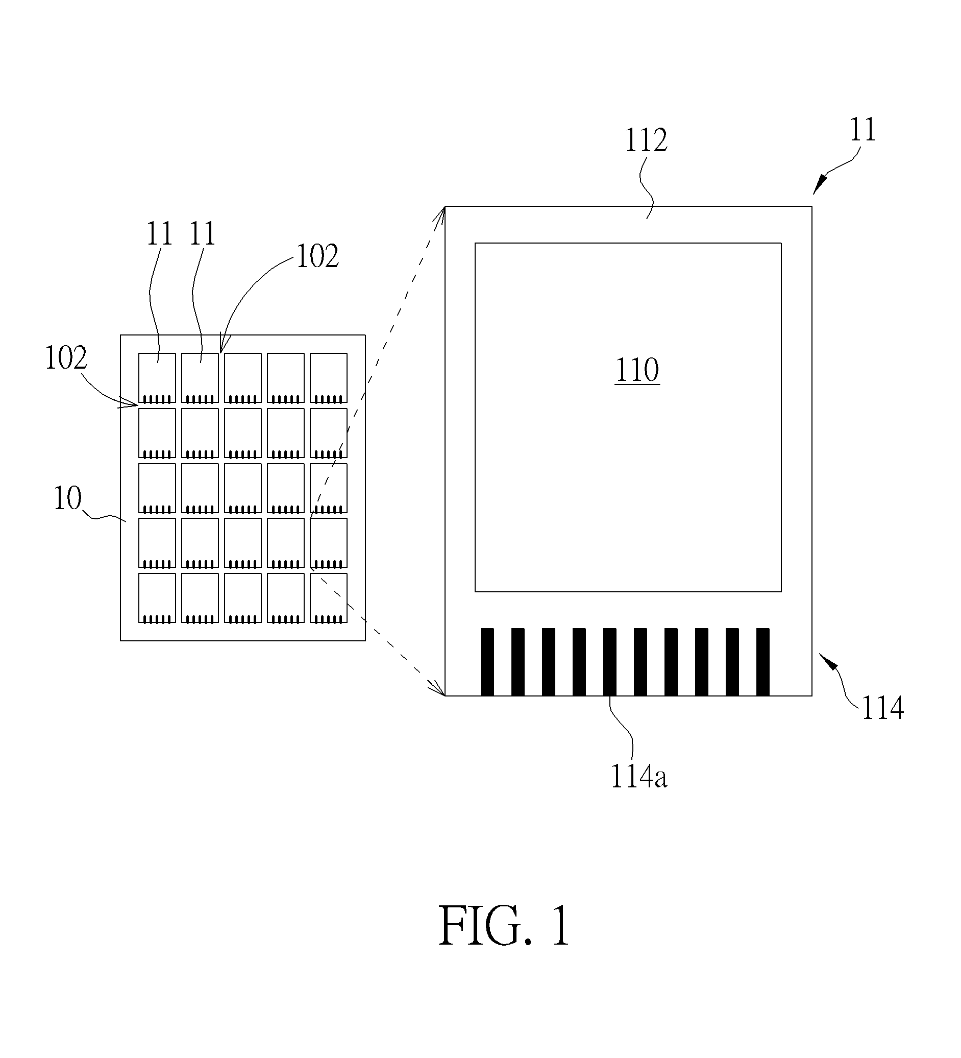
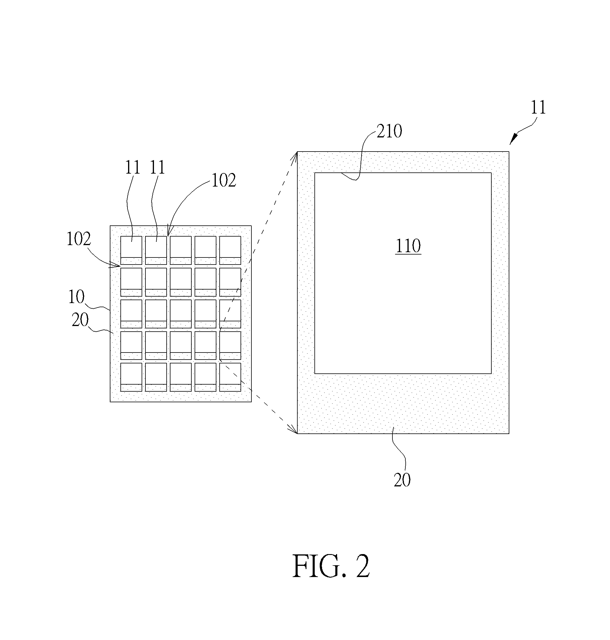
[0016]FIGS. 1-4 demonstrate a method of processing a panel or a substrate according to one embodiment of the invention.
[0017]First, as shown in FIG. 1, a substrate 10, such as a sensor substrate of a touch panel device, is provided. A plurality of chips 11 in an array (in this example to 5×5 array arrangement) is provided on the substrate 10. The chips 11 are separated from one another by a cutting lane 102.
[0018]According to the embodiment of the invention, the aforesaid substrate 10 may comprise a transparent substrate and at least one sensor electrode layer (not shown), but not limited thereto.
[0019]The aforesaid transparent substrate may comprise a polyethylene terephthalate (PET) substrate or a glass substrate, but not limited thereto.
[0020]The aforesaid sensor electrode layer may comprise indium tin oxide (ITO) transparent electrode, but not limited thereto.
[0021]As can be seen in the enlarged area in FIG. 1, each of the chips 11 may comprise an active area 110, a peripheral a...
PUM
| Property | Measurement | Unit |
|---|---|---|
| Fraction | aaaaa | aaaaa |
| Fraction | aaaaa | aaaaa |
| Thickness | aaaaa | aaaaa |
Abstract
Description
Claims
Application Information