

Image sensor structure
a sensor and image technology, applied in the direction of semiconductor devices, semiconductor/solid-state device details, electrical devices, etc., can solve the problems of inconvenient, even impossible, and achieve the effect of reducing the volume of the structure, facilitating packaging, and reducing the manufacturing cos
- Summary
- Abstract
- Description
- Claims
- Application Information
AI Technical Summary
Benefits of technology
Problems solved by technology
Method used
Image

Examples
Embodiment Construction
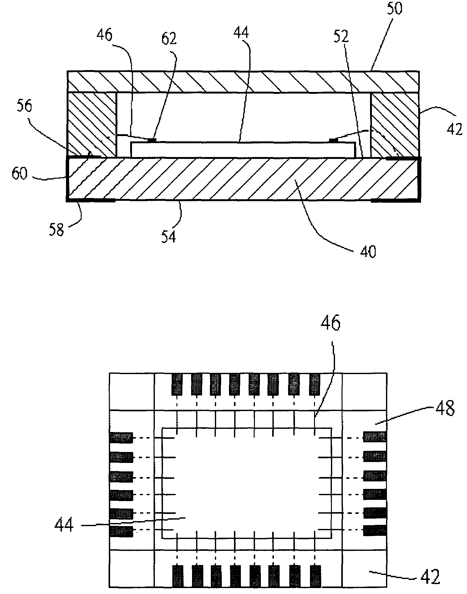
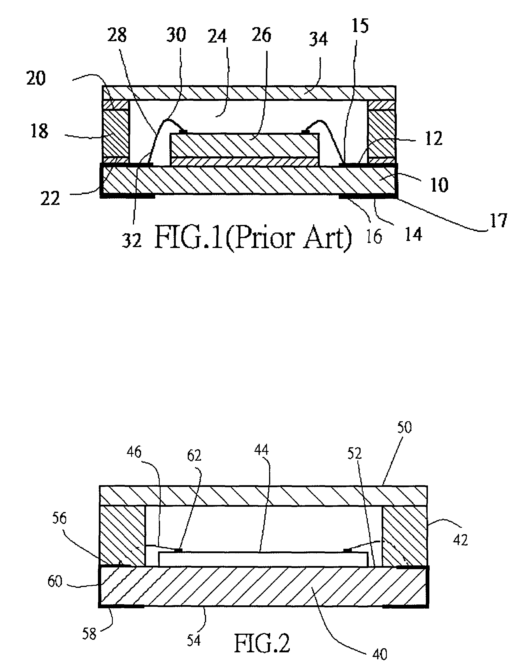
[0014]Please refer to FIG. 2, it is an image sensor structure of the present invention includes a substrate 40, four posts 42, a photosensitive chip 44, a plurality of wires 46, a glue layer 48, and a transparent layer 50.
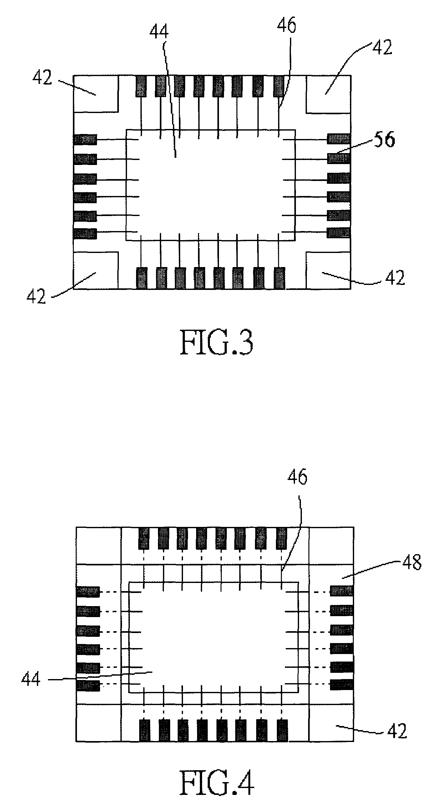
[0015]Please refer to FIG. 3 and FIG. 4. The substrate 40 has an upper surface 52 on which first electrodes 56 are formed, and a lower surface 54 on which second electrodes 58 are formed. Conductive elements 60 are formed on the periphery of the substrate 40 for electrically connecting the first electrodes 56 to corresponding to the second electrodes 58 of the substrate 40.
[0016]The four posts 42 are arranged on the four angle of the upper surface 52 of the substrate 40 individually.
[0017]The photosensitive chip 44 is mounted on the upper surface 52 of the substrate 40, a plurality of pads 62 are formed on the photosensitive chip 44.
[0018]The plurality of wires 46 are electrically connected the pads 62 of the photosensitive chip 44 to the first electrodes 56 of the...
PUM
 Abstract
Description
Claims
Application Information