Resistive touch screen having conductive mesh

a technology of resistive touch screen and conductive mesh, which is applied in the direction of electronic switching, pulse technique, instruments, etc., can solve the problems of reducing the clarity reducing the accuracy of the touch screen, and limited materials for spacer dots, etc., and achieves greater accuracy, robustness and clarity, and simple manufacturing.

Active Publication Date: 2007-03-27
EASTMAN KODAK CO
View PDF15 Cites 60 Cited by
  • Summary
  • Abstract
  • Description
  • Claims
  • Application Information

AI Technical Summary

Problems solved by technology

This process is relatively complex and expensive and the use of an additional material such as an adhesive can be expected to diminish the clarity of the touch screen.
Such prior art spacer dots are limited in materials selections to polymers that can be manufactured into small beads or UV coated from monomers.
In these prior art methods, the spacer dots may come loose and move around within the device, thereby causing unintended or inconsistent actuations.
Furthermore, contact between the conductive layers 14 and 18 is not possible where the spacer dots are located, thereby reducing the accuracy of the touch screen, and stress at the locations of the spacer dots can cause device failure after a number of actuations.
Unless steps are taken to adjust the index of refraction of the spacer dots, they can also be visible to a user, thereby reducing the quality of a display located behind the touch screen.
However, ITO tends to crack when stressed and conductive polymers may lack physical robustness and durability when stressed.
Moreover, when ITO is employed the thickness of the coating required to provide adequate durability limits the transparency and resistivity.
Such requirements add complexity to the manufacturing process, and may negatively impact yields.
Further, these approaches may not adequately electrically isolate the insulating islands, and will have reduced lifetime due to stresses induced in the cover sheet.
Moreover, the dimples on the back side of the cover sheet are objectionable or, if filled, require additional materials and manufacturing steps to fill.

Method used


Image

  • Resistive touch screen having conductive mesh
  • Resistive touch screen having conductive mesh
  • Resistive touch screen having conductive mesh

Examples


Embodiment Construction

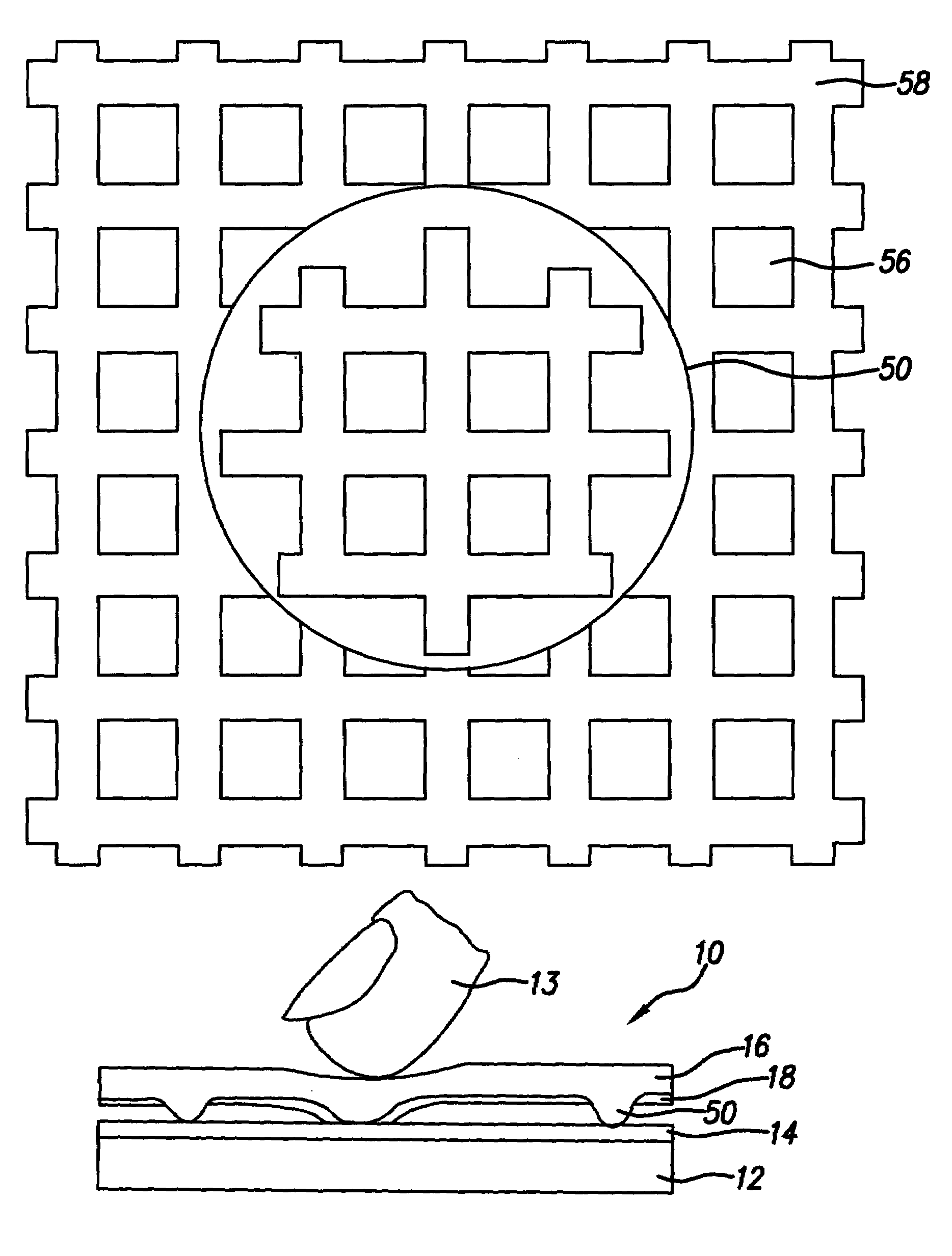
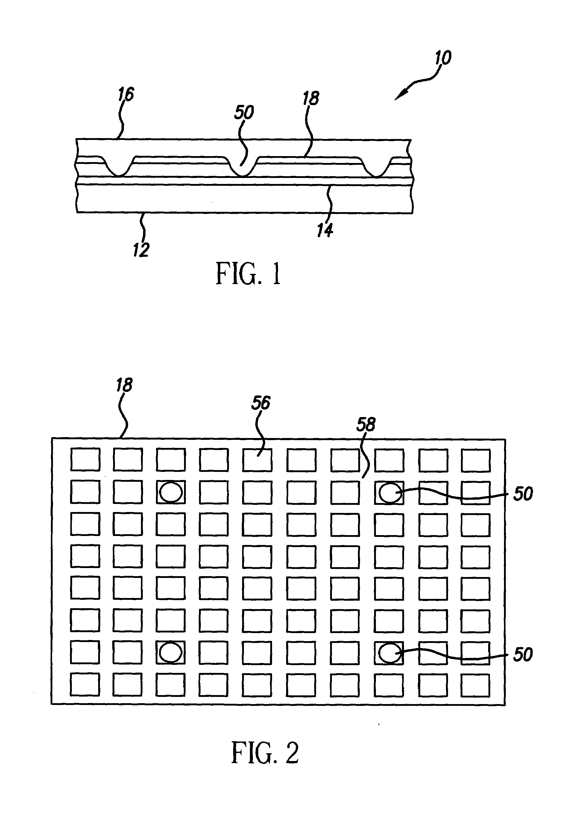
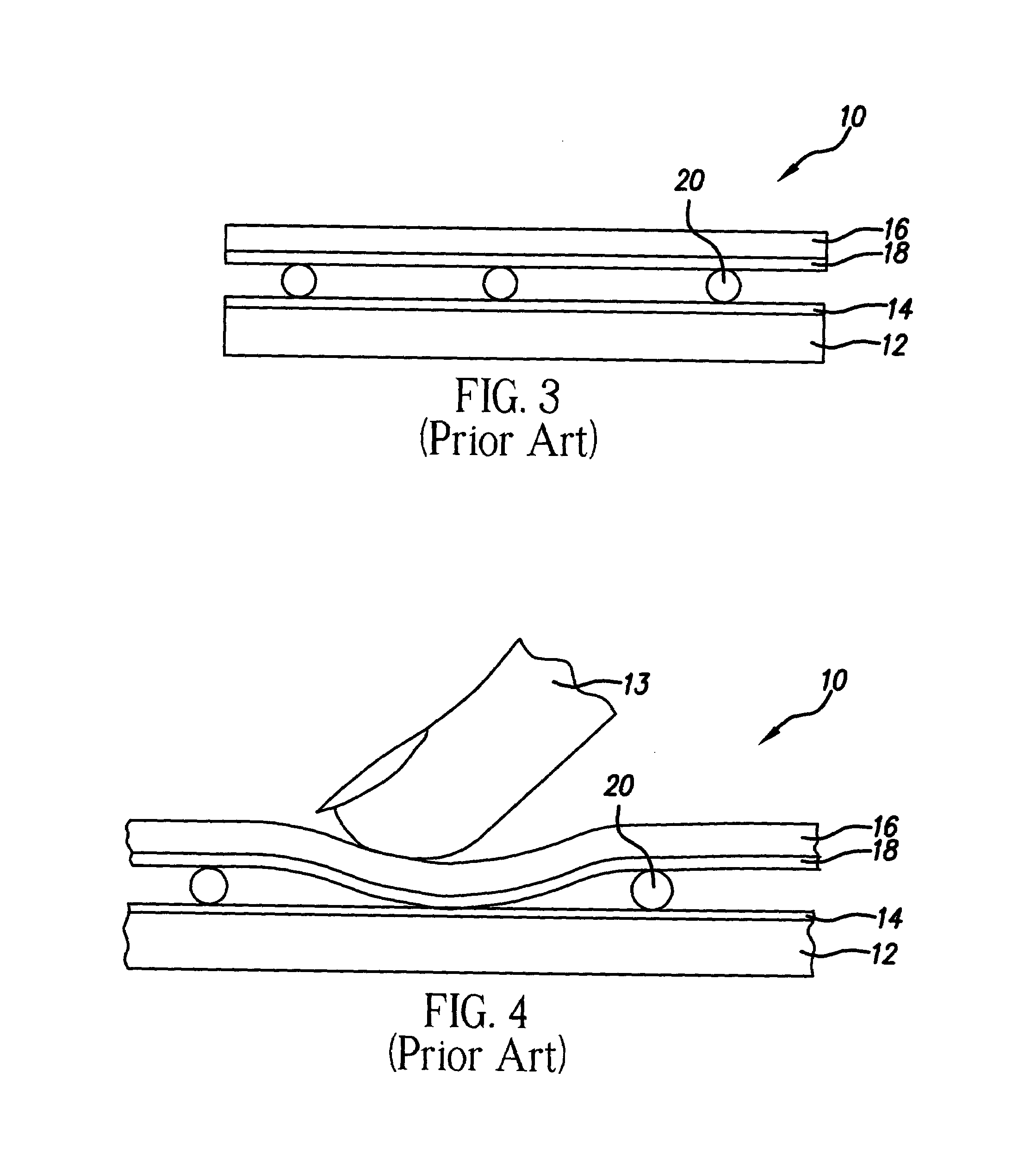
[0022]Referring to FIG. 1, the problems of the prior-art resistive touch screens are overcome through the use of a flexible cover sheet 16 having a second conductive layer 18 and integral compressible spacer dots 50 formed in the flexible cover sheet 16. Flexible cover sheet 16 comprises a substantially planar surface and the integral compressible spacer dots 50 are formed thereon, each integral compressible spacer dot having a base closest to the planar surface and a peak furthest from the planar surface. A second conductive layer 18 is coated over the flexible transparent cover sheet 16 between the spacer dots 50, but does not cover the peaks of the integral compressible spacer dots 50. The peaks of the integral compressible spacer dots 50 are located in non-conductive openings in the second conductive layer 18, whereby, when a force is applied to the flexible cover sheet 16 at the location of one of the integral compressible spacer dots 50, the integral compressible spacer dot is...


PUM

PropertyMeasurementUnit
diameteraaaaaaaaaa
transparencyaaaaaaaaaa
diameteraaaaaaaaaa

Abstract

A touch screen comprising: a) a substrate; b) a first conductive layer located on the substrate; c) a flexible sheet comprising a substantially planar surface and integral compressible spacer dots formed thereon, each integral compressible spacer dot having a base closest to the planar surface and a peak furthest from the planar surface; and d) a second conductive layer located on the surface of the flexible sheet, wherein the second conductive layer comprises a conductive mesh pattern and the peaks of the integral compressible spacer dots are located in non-conductive openings in the conductive mesh pattern; wherein when a minimum required activation force is applied to the touch screen at the location of one of the compressible spacer dots, the compressible spacer dot is compressed to allow electrical contact between the first and second conductive layers.

Description

FIELD OF THE INVENTION[0001]This invention relates to resistive touch screens and more particularly, to a flexible cover sheet and spacer dots separating the cover sheet from a substrate in a resistive touch screen.BACKGROUND OF THE INVENTION[0002]Resistive touch screens are widely used in conventional CRTs and in flat-panel display devices in computers and in particular with portable computers.[0003]FIG. 3 shows a portion of a prior-art resistive touch screen 10 of the type shown in Published US Patent Application No. 2002 / 0094660A1, filed by Getz et al., Sep. 17, 2001, and published Jul. 18, 2002, which includes a rigid transparent substrate 12, having a first conductive layer 14. A flexible transparent cover sheet 16 includes a second conductive layer 18 that is physically separated from the first conductive layer 14 by spacer dots 20 formed on the second conductive layer 18 by screen printing[0004]Referring to FIG. 4, when the flexible transparent cover sheet 16 is deformed, for...

Claims


Application Information

Patent Timeline
Patent Type & Authority Patents(United States)
IPC IPC(8): H01H1/10
CPCG06F3/045Y10T29/49105
Inventor COK, RONALD S.MAJUMDAR, DEBASISIRVIN, JR., GLEN C.
Owner EASTMAN KODAK CO
Why Eureka
Try Eureka