Optical delay element

a delay element and optical technology, applied in the field of optical delay elements, can solve the problems of large size of optical devices, difficult to compact optical devices, and large volume of optical devices, and achieve the effect of reducing the volume of line defects and enlarge the wavelength region

Active Publication Date: 2007-07-10
RICOH KK +1
View PDF14 Cites 0 Cited by
  • Summary
  • Abstract
  • Description
  • Claims
  • Application Information

AI Technical Summary

Benefits of technology

[0045]Summarizing effects of the present invention, in a line defect optical waveguide of the related art, the third order dispersion curve is a monotonic function and has no extreme, and in a coupled defect optical waveguide of the related art, although zero points exist in the third order dispersion curve, the sign of the third order dispersion curve does not change. According to the present invention, in the line defect optical waveguide formed in a photonic crystal structure, zero points exist in the third order dispersion curve of the waveguide band of the line defect optical waveguide, and near the zero points, the sign of the dispersion changes. Therefore, the waveguide band of the line defect optical waveguide can be changed by reducing the volume of the line defect optical waveguide, or by setting the refractive index of the line defect optical waveguide different from the refractive index of the photonic crystal structure portion, or by arranging an additional structure near the line defect optical waveguide, and as a result, the group refractive index obtainable with the line defect optical waveguide can be increased with dispersion remaining at a low level, and this can enlarge the wavelength region in which the wavelength dispersion of the group refractive index is small. Hence, it is possible to provide an optical delay element including a line defect optical waveguide formed in a photonic crystal structure, which has a group refractive index sufficiently greater than the refractive index of the constituent materials, and has approximately constant or small wavelength dispersion of the group refractive index in a wavelength region for practical use.
[0046]Consequently, by using the optical delay element of the present invention, it is possible to obtain a compact optical delay element, which is not attained in the related art, and it is possible to construct an optical pulse delay element able to actively control these optical elements by changing the refractive index. This invention is preferable applicable to an optical routing apparatus, or an optical information processing device.

Problems solved by technology

At least in principle, all these operations can be carried out by light, but the problem that should be solved is the switching element.
For these reasons, the optical device requires large size, and it is difficult to make the optical device compact.
When using the line defect optical waveguide to delay optical pulses, however, if the wavelength dispersion of the group refractive index is too large, the refractive index varies even when the wavelength changes slightly, and this line defect optical waveguide is not suitable for use as an optical element.

Method used


Image

  • Optical delay element
  • Optical delay element
  • Optical delay element

Examples


first embodiment

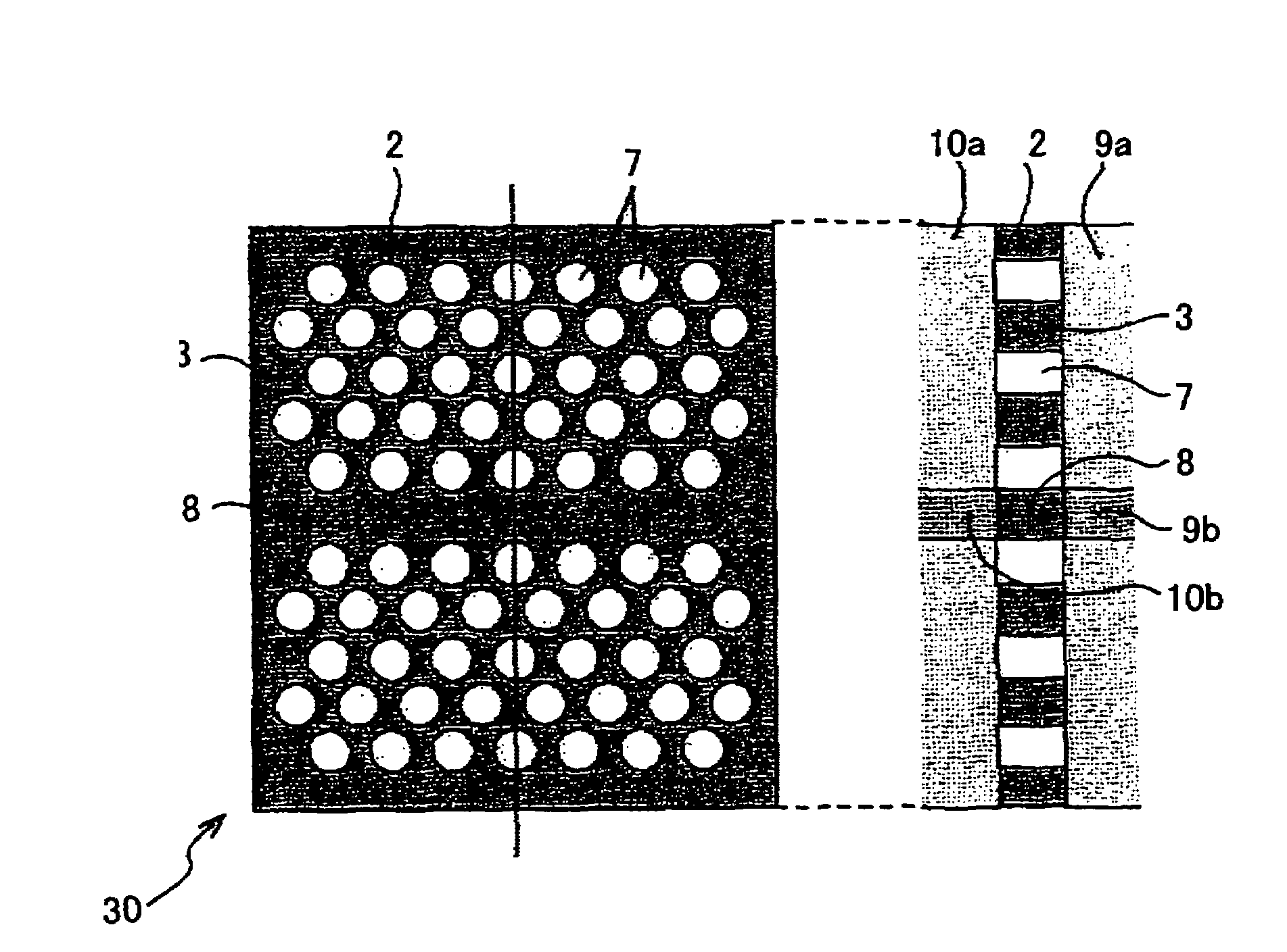
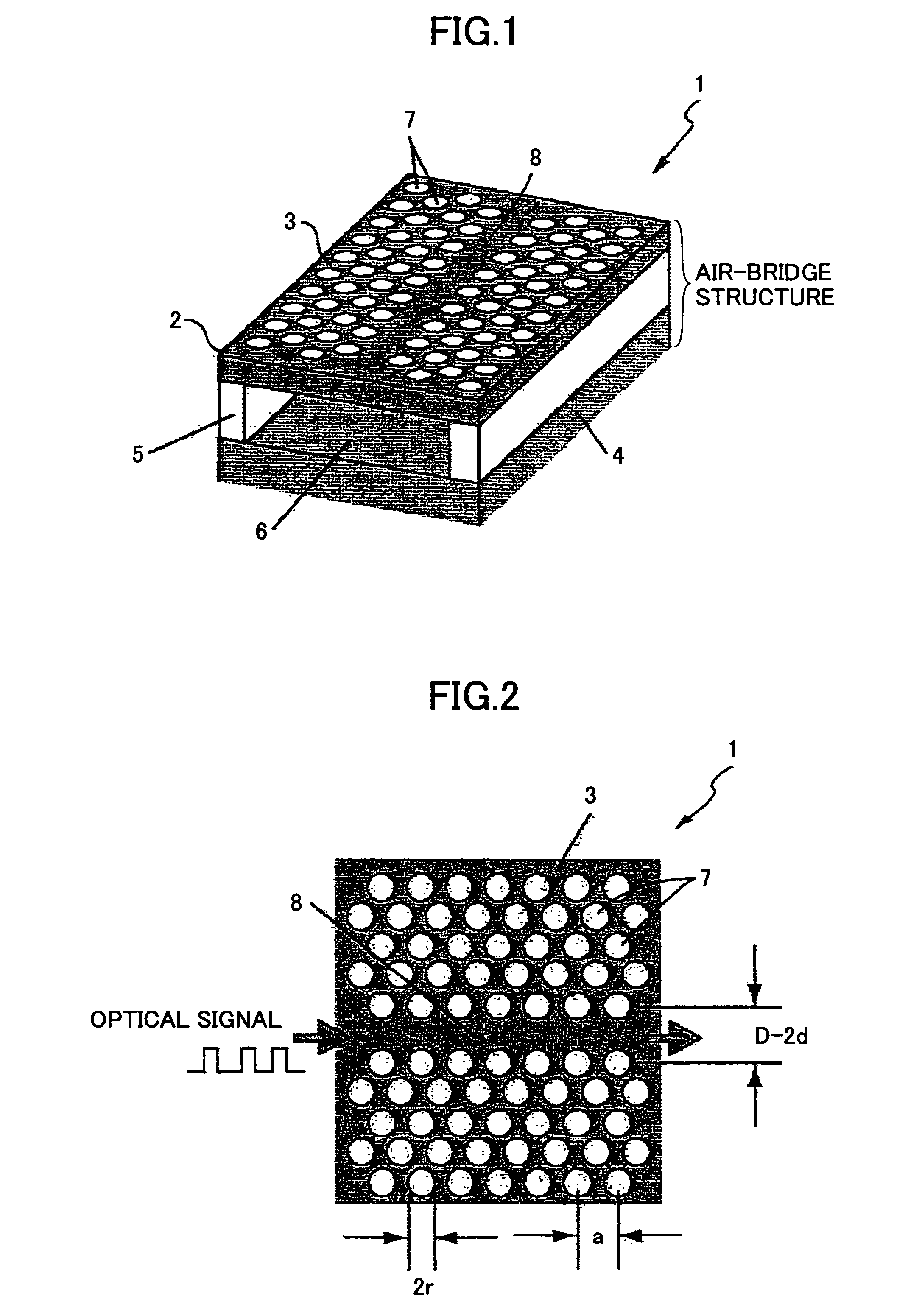
[0080]FIG. 1 is a perspective view for schematically illustrating an optical delay element 1 according to a first embodiment of the present invention, which includes a line defect optical waveguide formed from a two-dimensional photonic crystal slab.

[0081]FIG. 2 is a plan view of the optical delay element 1 in FIG. 1.

[0082]As illustrated in FIG. 1, the optical delay element 1 includes a substrate 4, pedestals 5 standing on the substrate 4, a high refractive index thin film 2 arranged on the pedestals 5, a cladding portion 6, which is actually an air space, and a photonic crystal structure 3 formed in the high refractive index thin film 2. For example, the thickness of the high refractive index thin film 2 is less than 1 μm. The photonic crystal structure 3 includes holes 7 filled with air. Because the cladding portion 6 is an air space, the structure of the optical delay element 1 is called an “air-bridge structure”.

[0083]If the refractive index of the high refractive index thin fil...

second embodiment

[0171]Expansion of a frequency region resulting in a large group refractive index, as described in the first embodiment, occurs even in a photonic crystal including a slab of a different refractive index.

[0172]In this embodiment, descriptions are made of an optical delay element in which the equivalent refractive index of the high refractive index thin film 2 is about two. In the present embodiment, the same reference numbers are assigned to the same elements as described in the previous embodiment, and overlapping descriptions are omitted.

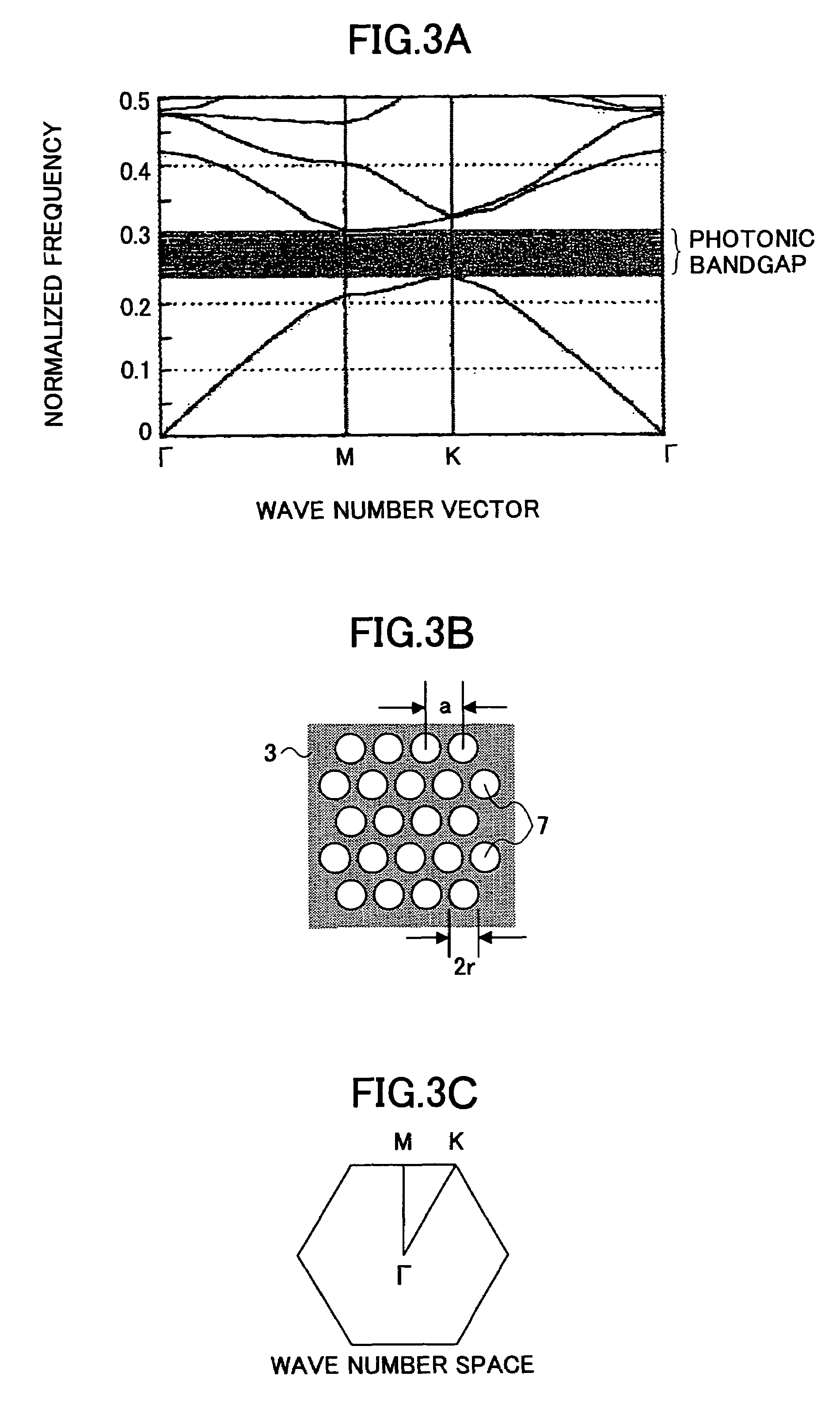
[0173]In a photonic crystal, if the contrast of refractive index is approximately two, a photonic bandgap appears in the photonic crystal. However, in the case of the two-dimensional photonic crystal slab structure, because of strong influences of light lines, design tolerance becomes small.

[0174]For example, a thin film substrate 2 having an equivalent refractive index near two is made, and the photonic crystal structure 3 constituted from the ai...

third embodiment

[0193]In this embodiment, a method is described of fabricating the optical delay element of the present invention. In the present embodiment, the same reference numbers are assigned to the same elements as described in the previous embodiment, and overlapping descriptions are omitted.

[0194]As described above, a two-dimensional photonic crystal can be fabricated with a SOI (silicon-on-insulator) substrate and semiconductor fine processing techniques.

[0195]With the latest SOI technology, a SOI substrate including a 0.2 μm-thick silicon layer is commercially available, and this SOI substrate can be used to fabricate the two-dimensional photonic crystal.

[0196]The triangular lattice of holes can be built by lithography and dry etching. For example, an electron-beam resist is applied on a substrate, then the resist is patterned by drawing circular holes having diameter of 400 nm in the resist with an electron beam. The diameter of the holes is decided by the object light wavelength of the...


PUM

PropertyMeasurementUnit
refractive indexaaaaaaaaaa
lengthaaaaaaaaaa
lengthaaaaaaaaaa

Abstract

An optical delay element including a photonic crystal line defect optical waveguide is disclosed that has a large group refractive index and has small or nearly constant wavelength dispersion of the group refractive index in a wide wavelength region for practical use. The optical delay element includes a line defect optical waveguide formed in a photonic crystal structure, and the volume of the line defect optical waveguide is less than the volume of a single line defect optical waveguide. Thereby, the waveguide band of the line defect optical waveguide has two zero points in the third order dispersion curve of the line defect optical waveguide, and the sign of the third order dispersion curve is inverted near the zero points. Therefore, the waveguide band of the line defect optical waveguide is modified, and this enables expansion of the wavelength region having a large group refractive index, small wavelength dispersion of the group refractive index, and small wavelength dispersion of the speed of optical pulses.

Description

BACKGROUND OF THE INVENTION[0001]1. Field of the Invention[0002]The present invention relates to an optical delay element using a photonic crystal.[0003]2. Description of the Related Art[0004]One of the subjects in optical communication is to provide an optical switching system able to change optical paths without opto-electric conversion of optical signals when transmitting optical packet data. In the related art, however, the optical signals have to be completely converted to electrical signals first, and then after the transmission paths are determined (changed) in form of electrical signals, the electrical signals are converted to optical signals again by electric-opto conversion.[0005]In order to transmit optical signals themselves, it is necessary to use a switching element for changing the polarization direction of the light beam being transmitted, and an element for analyzing the polarization direction of the light beam. In addition, in an optical packet, a header containing...

Claims


Application Information

Patent Timeline
Patent Type & Authority Patents(United States)
IPC IPC(8): G02B6/10G02B6/00G02B6/12G02B6/122G02F1/01G02F1/035G02F1/313G02F1/365
CPCB82Y20/00G02B6/1225
Inventor SAKAI, ATSUSHIKATOH, IKUOFUNATO, HIROYOSHIBABA, TOSHIHIKO
Owner RICOH KK
Why Eureka
Try Eureka