Eureka AIR delivers breakthrough ideas for toughest innovation challenges, trusted by R&D personnel around the world.

Dual layer stress liner for MOSFETS

a technology of mosfets and stress lines, which is applied in the direction of semiconductor devices, basic electric elements, electrical appliances, etc., can solve the problems of affecting the overall affecting the reliability of the transistor, and reducing reliability and performance in terms of thick gate oxide breakdown, so as to reduce the damage of high power

Inactive Publication Date: 2009-04-21
IBM CORP +1
View PDF6 Cites 3 Cited by
  • Summary
  • Abstract
  • Description
  • Claims
  • Application Information

AI Technical Summary

Benefits of technology

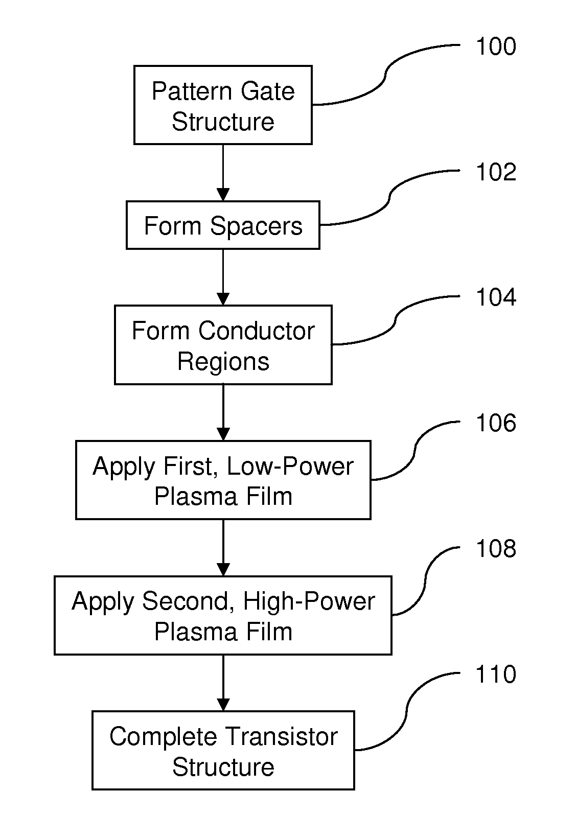
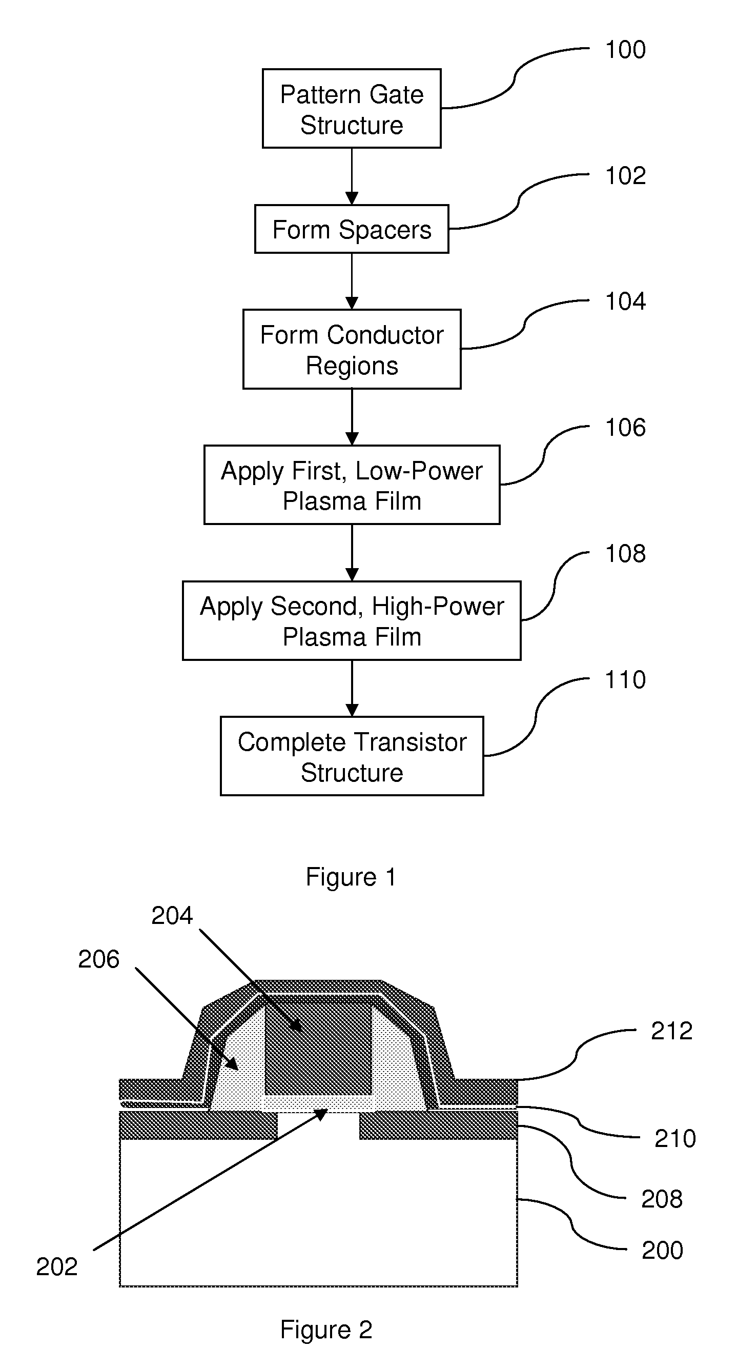
[0005]In view of the foregoing, an embodiment of the invention provides a method of producing a metal oxide semiconductor field effect transistor (MOSFET). The method creates a transistor by patterning a gate structure over a substrate, forming spacers on sides of the gate structure, and forming conductor regions within the substrate on alternate sides of the gate stack. The gate structure and the conductor regions make up the transistor. In order to reduce high power plasma induced damage, the method initially applies a first plasma having a first power level to the transistor to form a first stress layer over the transistor. After the first lower-power plasma is applied, the method then applies a second plasma having a second power level to the transistor to form a second stress layer over the first stress layer. The second power level is higher (e.g., at least 5 times higher) than the first power level.

Problems solved by technology

Modern day logic transistors are exposed to plasma damage at many stages of processing.
However, exposing transistors to high-power plasma processes can sometimes affect the overall reliability of the transistors.
In fact there is sometimes a remarkable decrease in reliability and performance in terms of thick gate oxide breakdown, enhanced bias temperature instability (NBTI), and other problems because of such high-power plasma-based films.

Method used


Image

  • Dual layer stress liner for MOSFETS
  • Dual layer stress liner for MOSFETS

Examples


Embodiment Construction

[0011]The embodiments of the invention and the various features and advantageous details thereof are explained more fully with reference to the non-limiting embodiments that are illustrated in the accompanying drawings and detailed in the following description. It should be noted that the features illustrated in the drawings are not necessarily drawn to scale. Descriptions of well-known components and processing techniques are omitted so as to not unnecessarily obscure the embodiments of the invention. The examples used herein are intended merely to facilitate an understanding of ways in which the embodiments of the invention may be practiced and to further enable those of skill in the art to practice the embodiments of the invention. Accordingly, the examples should not be construed as limiting the scope of the embodiments of the invention.

[0012]As mentioned above, transistors are exposed to potential plasma damage at many stages of processing. This plasma damage is aggravated due ...


PUM


Abstract

A method of producing a metal oxide semiconductor field effect transistor (MOSFET) creates a transistor by patterning a gate structure over a substrate, forming spacers on sides of the gate structure, and forming conductor regions within the substrate on alternate sides of the gate stack. The gate structure and the conductor regions make up the transistor. In order to reduce high power plasma induced damage, the method initially applies a first plasma having a first power level to the transistor to form a first stress layer over the transistor. After the first lower-power plasma is applied, the method then applies a second plasma having a second power level to the transistor to from a second stress layer over the first stress layer. The second power level is higher (e.g., at least 5 times higher) than the first power level.

Description

BACKGROUND[0001]1. Field of the Invention[0002]The embodiments of the invention generally relate to metal oxide semiconductor field effect transistors (MOSFETS), and, more particularly, to an improved method of forming a stressing layer without damaging the underlying transistor and without compromising its performance.[0003]2. Description of the Related Art[0004]Modern day logic transistors are exposed to plasma damage at many stages of processing. This plasma damage is aggravated due to the usage of more plasma processing steps, such as with the introduction of plasma generated stress liners which improve logic performance by carrier hole mobility enhancement. High-power high density plasma-based films (HDP) have an advantage over conventional plasma enhanced chemical vapor deposition (PECVD) films, because they reduce the performance offset between isolated and nested devices. However, exposing transistors to high-power plasma processes can sometimes affect the overall reliabilit...

Claims


Application Information

Patent Timeline
Patent Type & Authority Patents(United States)
IPC IPC(8): H01L21/8238
CPCH01L21/31604H01L29/66575H01L29/7843H01L21/02263H01L21/02107H01L21/76832
Inventor NAIR, DELEEP R.BAIOCCO, CHRISTOPHER V.CHEN, XIANGDONGKIM, JUNJUNGPARK, JAE-EUNYANG, DAEWON
Owner IBM CORP
Why Eureka
Eureka Blog
Learn More