Demodulation circuit and demodulating method

a demodulation circuit and digital modulation technology, applied in the direction of pulse technique, transmission monitoring, phase-modulated carrier system, etc., can solve the problem of not being able to capture the carrier

Inactive Publication Date: 2010-04-13
FUJITSU SEMICON LTD
View PDF7 Cites 0 Cited by
  • Summary
  • Abstract
  • Description
  • Claims
  • Application Information

AI Technical Summary

Benefits of technology

[0048]According to the present invention, when the phase advance or delay of a carrier wave cannot be discriminated, the integrated value of a loop filter can reach the maximum integrated value on the phase-advance determined side by determining as a phase advance. When the integrated value of the loop filter reaches the maximum integrated value on the phase-advance determined side, the integrated value can be shifted to the maximum integrated value on the phase-delay determined side. Thus, the capture range of the carrier wave regeneration loop can be broad, and the capture time can be shortened.
[0050]According to the present invention, when the phase advance or delay of a carrier wave cannot be discriminated, the integrated value of a loop filter can reach the maximum integrated value on the phase-delay determined side by determining such status as a phase delay. When the integrated value of the loop filter reaches the maximum integrated value on the phase-delay determined side, the integrated value can be shifted to the maximum integrated value on the phase-advance determined side. Thus, the capture range of the carrier wave regeneration loop can be broad, and the capture time can be shortened.
[0052]With the above-mentioned configuration, although the signal points of a carrier wave exist at random on the I and Q phase plane, a predetermined value indicating a phase determination result other than 0 is output relative to a signal point on a predetermined line or in a predetermined area, thereby allowing the integrated value of the loop filter to reach the maximum integrated value on the phase-advance determined side or the maximum integrated value on the phase-delay determined side.
[0058]According to the present invention, when the phase advance or delay of a clock cannot be discriminated, the integrated value of a loop filter can reach the maximum integrated value on the phase-advance determined side by determining such status as a phase advance. When the integrated value reaches the maximum integrated value on the phase-advance determined side, the integrated value can be shifted to the maximum integrated value on the phase-delay determined side. Thus, the capture range of the clock regeneration loop can be broad, and the capture time can be shortened.
[0060]According to the present invention, when the phase advance or delay of a symbol timing cannot be discriminated, the integrated value of a loop filter can reach the maximum integrated value on the phase-delay determined side. When the integrated value reaches the maximum integrated value on the phase-delay determined side, the integrated value of the loop filter can be shifted to the maximum integrated value on the phase-advance determined side. Thus, the capture range of the clock regeneration loop can be broad, and the capture time can be shortened.

Problems solved by technology

Therefore, there has been the problem that, like the above-mentioned timing recovery loop, the output of the loop filter 42 is fixed to a specific value, and no carrier can be captured.

Method used


Image

  • Demodulation circuit and demodulating method
  • Demodulation circuit and demodulating method
  • Demodulation circuit and demodulating method

Examples


first embodiment

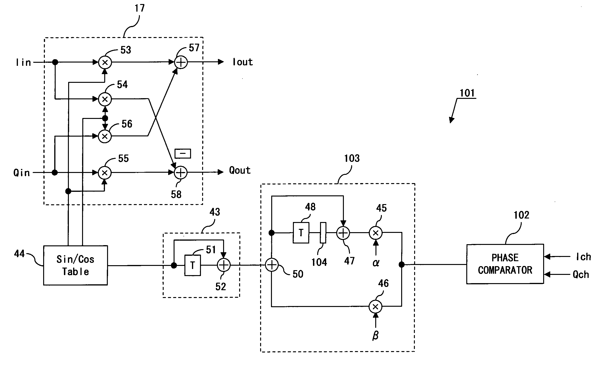
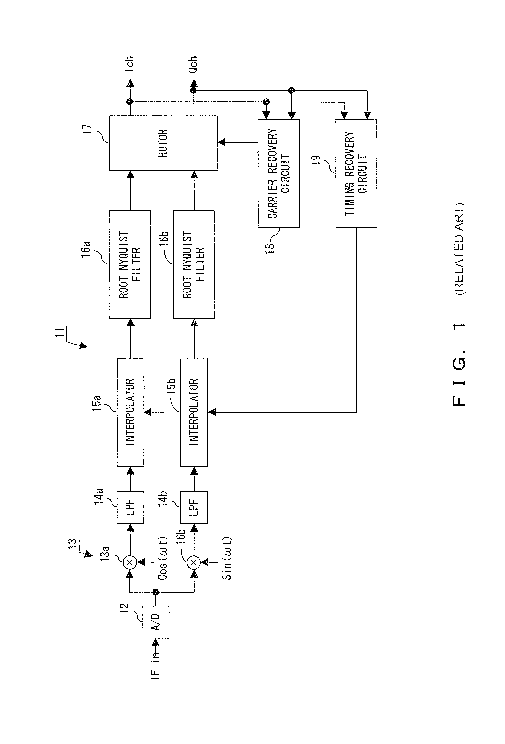
[0083]FIG. 8 shows the configuration of the carrier recovery loop of the digital demodulation circuit according to the present invention. In FIG. 8, the circuit block that is the same as the carrier recovery loop shown in FIG. 6 is assigned the same reference numeral, and the detailed explanation is omitted here. In the circuit shown in FIG. 8, the differences from the circuit shown in FIG. 6 are the configurations of a phase comparator 102 and a loop filter 103 in a carrier recovery circuit 101.

[0084]FIG. 9 shows the configuration of the phase comparator 102 in the carrier recovery circuit 101.

[0085]The phase comparator (corresponding to the phase error determination circuit) 102 comprises a polarity extraction circuit 111 for extracting the polarity of an I channel signal (Ich, hereinafter referred to as an I signal), a polarity extraction circuit 112 for extracting the polarity of a Q channel signal (Qch, hereinafter referred to as a Q signal), a multiplier 113 for multiplying th...

second embodiment

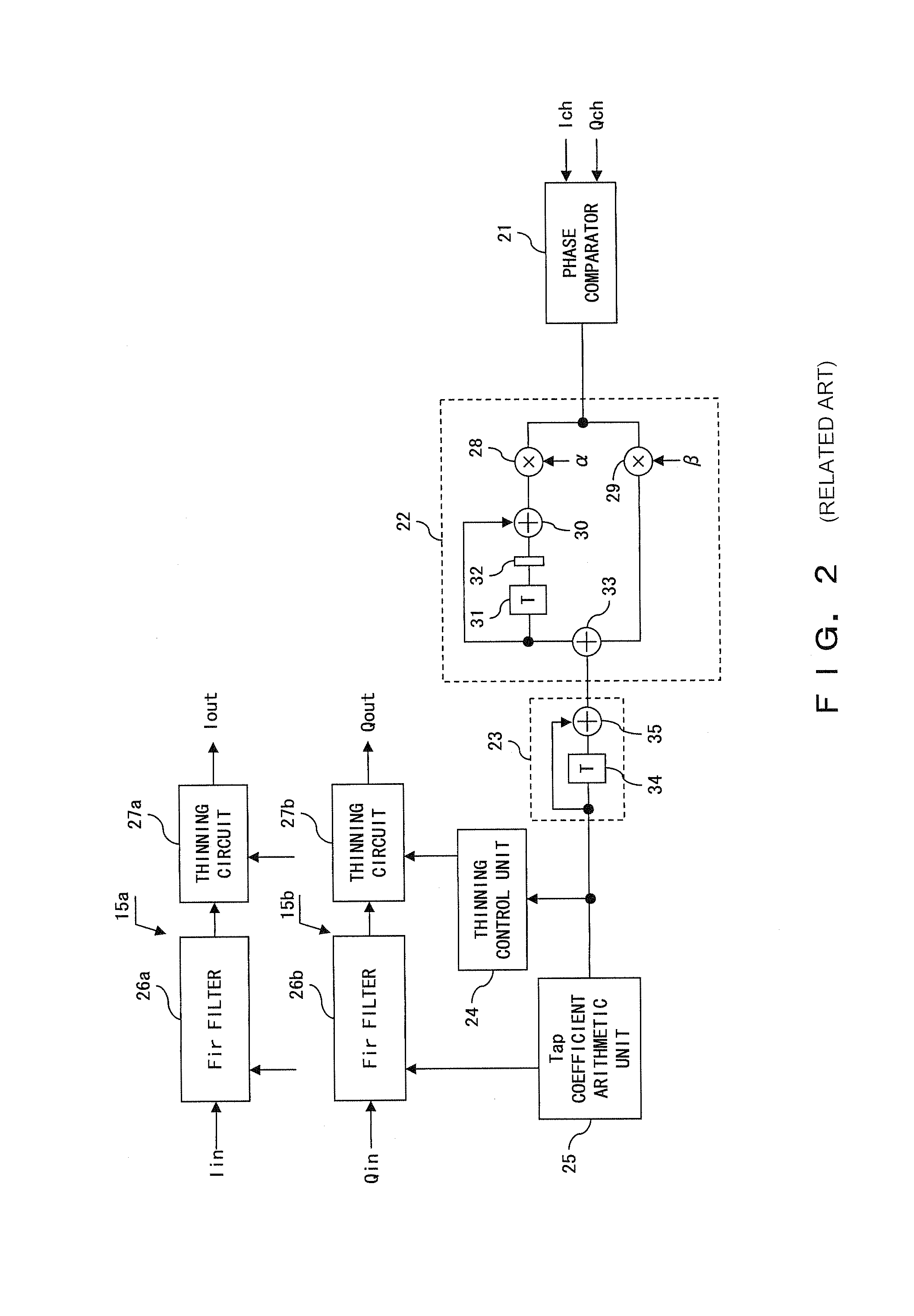
[0102]The operation performed during the synchronous capture of the carrier recovery loop is explained by referring to the flowchart shown in FIG. 11. The synchronous capturing operation of the timing recovery loop according to the present invention is the same as the process shown in FIG. 11.

[0103]The carrier recovery loop performs the synchronous capturing process of the carrier of a received signal (S11 shown in FIG. 11).

[0104]The limiter 104 determines whether or not the output of the adder 30 (hereinafter referred to as a value of an integrator) is equal to or larger than the positive maximum value Lim_max (S12). The process corresponds to the function of the comparator 201 of the limiter 104.

[0105]When the value of the integrator is equal to or larger than the positive maximum value Lim_max (YES in S12), control is passed to step S13, “−(Lim_max-Lim_min)” is added to the current value of the integrator, and the sum is output to the integrator 48. The process corresponds to the...


PUM


Abstract

A demodulation circuit can perform a capturing operation although a frequency error is large. A phase comparator out puts a predetermined value other than 0 as a determination result of a phase error when a phase error of a carrier wave is large and a signal point is located at a predetermined position. A loop filter outputs a negative minimum value to an integrator when an integrated value of a determination result reaches a positive maximum value of a limiter. Thus, when a phase error is large, a value changing from a negative minimum value to a positive maximum value is output from the loop filter, thereby realizing a broad synchronous capture range.

Description

CROSS-REFERENCE TO RELATED APPLICATIONS[0001]This application is based upon and claims the benefit of priority from the prior Japanese Patent Application No. 2006-013205 filed on Jan. 20, 2006, the entire contents of which are incorporated herein by reference.BACKGROUND OF THE INVENTION[0002]1. Field of the Invention[0003]The present invention relates to a demodulation circuit and a demodulating method for demodulating a digital-modulated signal.[0004]2. Description of the Related Art[0005]FIG. 1 is a block diagram of a common QPSK demodulation circuit. A QPSK-modulated signal is received by a tuner not shown in the attached drawings, and converted into an intermediate frequency signal IFin. The intermediate frequency signal IFin is converted by an A / D converter 12 into digital data at the timing synchronous with the sampling clock with a predetermined frequency, and further converted by an IQ separator 13 into a baseband signal formed by an I signal and a Q signal.[0006]The IQ sepa...

Claims


Application Information

Patent Timeline
Patent Type & Authority Patents(United States)
IPC IPC(8): H04L27/00
CPCH04L7/0054H04L27/2067H04L7/0029H04L2027/0079H04L2027/0057H04L2027/0067H04L2027/0032H04L27/38H04L27/22
Inventor KITTA, TATSUAKIIWAMATSU, TAKANORI
Owner FUJITSU SEMICON LTD
Why Eureka
Try Eureka