Memory controller, nonvolatile storage device, nonvolatile storage system, and data writing method

a memory controller and storage device technology, applied in the field of memory controllers, can solve the problems of time-consuming processing and complicated techniques, and achieve the effect of high speed

Inactive Publication Date: 2010-04-20
PANASONIC CORP
View PDF16 Cites 83 Cited by
  • Summary
  • Abstract
  • Description
  • Claims
  • Application Information

AI Technical Summary

Benefits of technology

[0036]According to the present invention, in writing data to the main storage memory given from the outside, it becomes possible to rationalize the saving processing and thereby perform the data writing at a high speed by temporarily storing the data in the auxiliary storage memory (buffering), collectively taking out a plurality of pieces of data in the auxiliary storage memory, and then storing them in the main storage memory. Moreover, since new data is written in the auxiliary storage memory based on a completion state of the data writing to the main storage memory etc., it is possible to write the data surely even when abnormalities take place, such as a writing error in the main storage memory and the power shutdown of the storage device.

Problems solved by technology

As is clear from the above explanation, since the “rewriting technique on the premise of saving data” is such that un-rewritten data is temporarily saved in another physical block although it is the rewriting of one cluster, subsequently new data is written in the physical block, and the physical block previously being used is erased, the technique is complicated and time-consuming processing.

Method used


Image

  • Memory controller, nonvolatile storage device, nonvolatile storage system, and data writing method
  • Memory controller, nonvolatile storage device, nonvolatile storage system, and data writing method
  • Memory controller, nonvolatile storage device, nonvolatile storage system, and data writing method

Examples


first embodiment

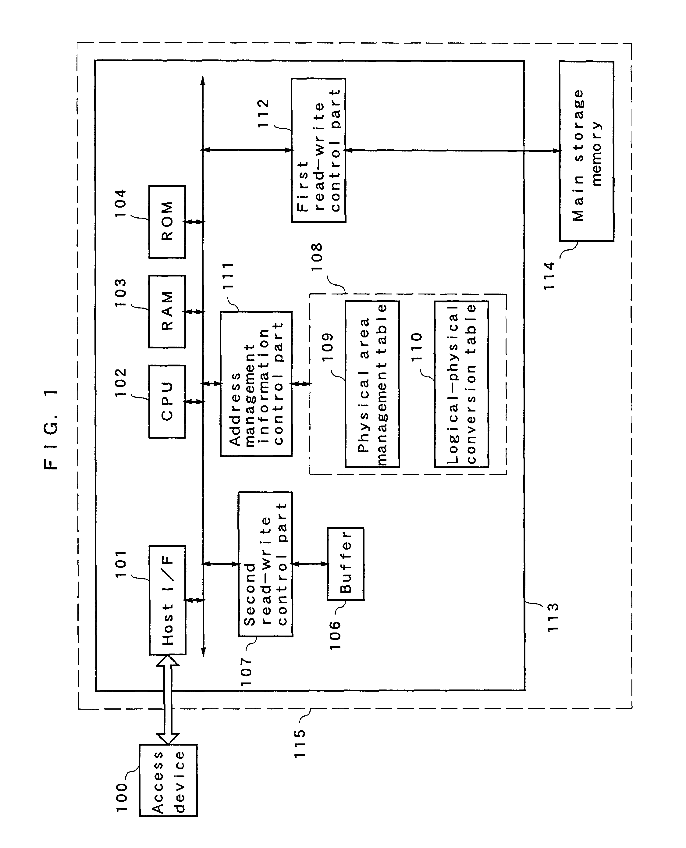
[0068]Hereafter, a nonvolatile storage system according to the present invention will be explained. FIG. 1 is a block diagram of the nonvolatile storage system. The nonvolatile storage system includes a nonvolatile storage device and an access device 100 to which the nonvolatile storage device is connected.

[0069]A nonvolatile storage device 115 has a memory controller 113 and nonvolatile main storage memory 114 composed of a flash memory, and is capable of accessing the access device 100 provided outside.

[0070]The access device 100 performs transmission of read and write commands for user data (hereinafter simply referred to as data) and a logical address at which the data is stored and transmission and reception of the data, for the main storage memory 114 through the memory controller 113. In response to the read and write commands from this access device 100, the memory controller 113 writes the received data into the main storage memory 114, and reads the data from the main stor...

second embodiment

[0185]Next, a nonvolatile storage system according to the present invention will be explained.

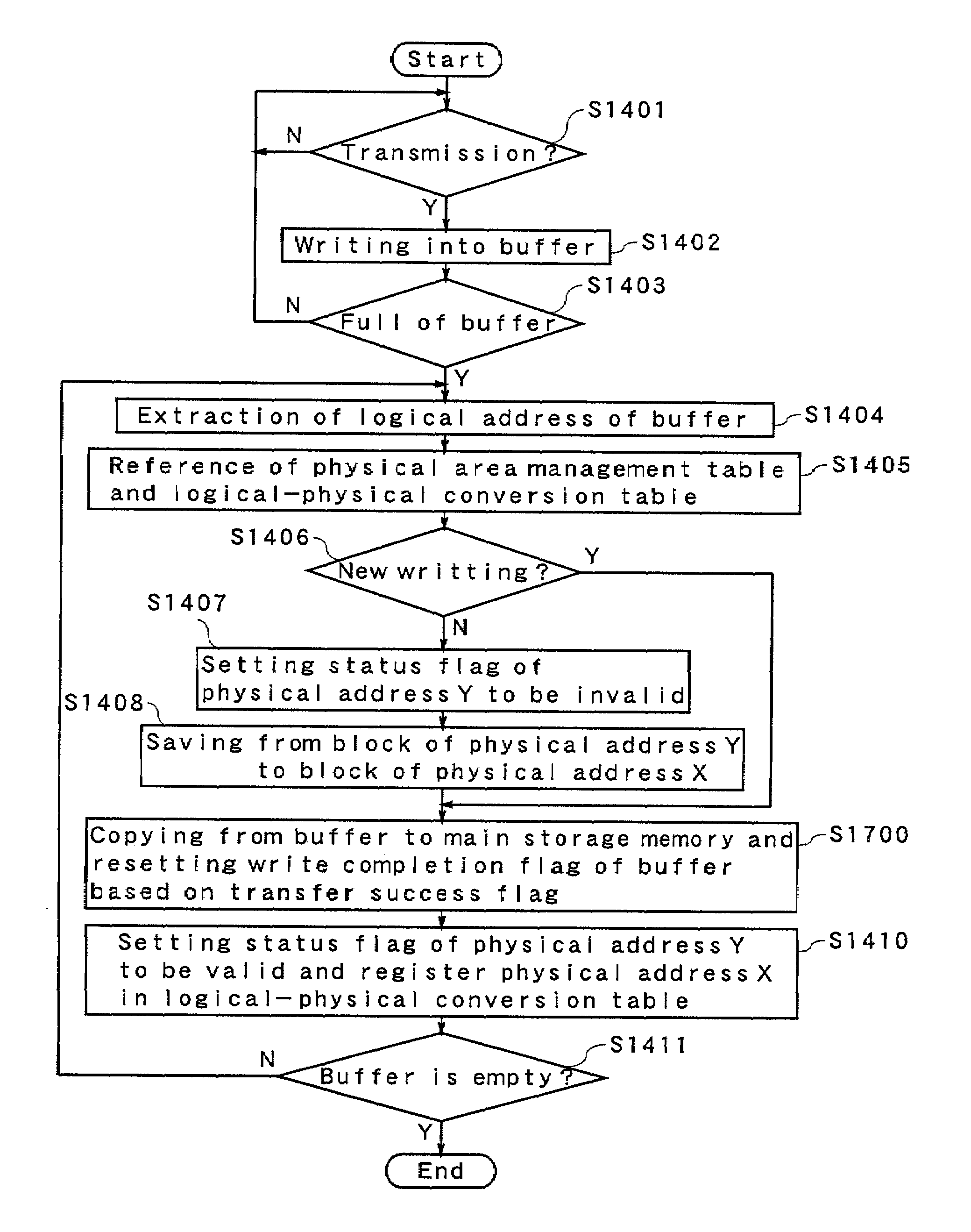
[0186]The present embodiment differs largely from the first embodiment in that, when data of two clusters temporarily stored in the buffer 106 is collectively written in the main storage memory 114, a “transfer success flag” is created based on a “write completion signal (ready / busy signal)” and a “status signal” outputted from the main storage memory 114, and it is determined whether new data transferred from the access device 100 can be overwritten in the buffer 106 based on the transfer success flag.

[0187]FIG. 16 is a block diagram of the nonvolatile storage system according to the present embodiment.

[0188]In a case of the present embodiment, the main storage memory 114 outputs a write completion signal indicating that the data writing to the main storage memory 114 is completed to a system bus. If the value of the write completion signal is 0, the data is being written in the main stora...


PUM


Abstract

A nonvolatile storage device is provided with a nonvolatile main storage memory whose erase size is larger than a cluster size, and a buffer, i.e. a nonvolatile auxiliary storage memory. At the time of writing data in the memory, the data is temporarily stored in the buffer, then, a plurality of data in the buffer are collectively taken out to be stored in the main storage memory. Data in an original block is saved in a write block in the main storage memory. Thus, the data can be written in the main storage memory at a high speed.

Description

TECHNICAL FIELD[0001]The present invention relates to a nonvolatile storage device, such as a semiconductor memory card including a flash memory as a main storage memory thereof, and a memory controller built therein. Furthermore, the present invention also includes a nonvolatile storage system adding an access device to the nonvolatile storage device as its constituent element, and a data writing method that describes operations of the memory controller.BACKGROUND ART[0002]Demands of the nonvolatile storage device including a nonvolatile main storage memory capable of rewriting widely spread mainly in the semiconductor memory card. Such semiconductor memory cards include various types, and as one of them, there is a SD memory card (registered trademark). This SD memory card includes a flash memory as a nonvolatile main storage memory, and has a memory controller for controlling it. The memory controller is configured to perform read-write control on the flash memory in response to ...

Claims


Application Information

Patent Timeline
Patent Type & Authority Patents(United States)
IPC IPC(8): G06F12/12
CPCG06F3/0613G06F3/0619G06F3/0643G06F3/0679G06F12/0246G06F3/0656G06F2212/7203G06F2212/1016
Inventor NAKANISHI, MASAHIROIZUMI, TOMOAKIKASAHARA, TETSUSHITAMURA, KAZUAKIMATSUNO, KIMINORINAKAMURA, YUTAKATOYAMA, MASAYUKIGOHO, YASUSHIIWANARI, SYUNICHIKATO, YOSHIHISAINOUE, MANABU
Owner PANASONIC CORP
Why Eureka
Try Eureka