Supercharge Your Innovation With Domain-Expert AI Agents!

Semiconductor package system with thermal die bonding

a technology of thermal die bonding and semiconductor, applied in the direction of semiconductor/solid-state device details, semiconductor devices, electrical devices, etc., can solve the problems of adverse effect on the performance and reliability of semiconductors, and insufficient heat dissipation properties

Active Publication Date: 2010-05-11
STATS CHIPPAC LTD
View PDF11 Cites 5 Cited by
  • Summary
  • Abstract
  • Description
  • Claims
  • Application Information

AI Technical Summary

Benefits of technology

This system provides enhanced heat dissipation capabilities, controlling thermal performance through design patterns and using less expensive adhesives, while maintaining compatibility with conventional manufacturing technologies, thus addressing the limitations of prior solutions.

Problems solved by technology

The heat spreader thereby removes the heat from the semiconductor and reduces the likelihood of the occurrence of hot spots that can have an adverse effect on the performance and reliability of the semiconductor.
However, even with a multilayer circuit board using a metal sheet for a core substrate, the heat-dissipating properties are not always enough considering the increasing amount of heat generated from a semiconductor element, and a multilayer circuit board having better heat-dissipating properties is required to remove the heat generated from a semiconductor element.
Again, with a multilayer circuit board using such a cover member, heat-dissipating properties are not always enough to increase amount of heat removed from a semiconductor element, and a multilayer circuit board having improved heat-dissipating properties is again required.
In these cases, the material cost is increased around double compared with conventional epoxy material.
At the same time, it is very hard to get stable workability and reliable performance with these packages.
Solutions to these problems have been long sought but prior developments have not taught or suggested any solutions and, thus, solutions to these problems have long eluded those skilled in the art.

Method used


Image

  • Semiconductor package system with thermal die bonding
  • Semiconductor package system with thermal die bonding
  • Semiconductor package system with thermal die bonding

Examples


Embodiment Construction

[0027]In the following description, numerous specific details are given to provide a thorough understanding of the invention. However, it will be apparent that the invention may be practiced without these specific details. In order to avoid obscuring the present invention, some well-known circuits, system configurations, and process steps are not disclosed in detail.

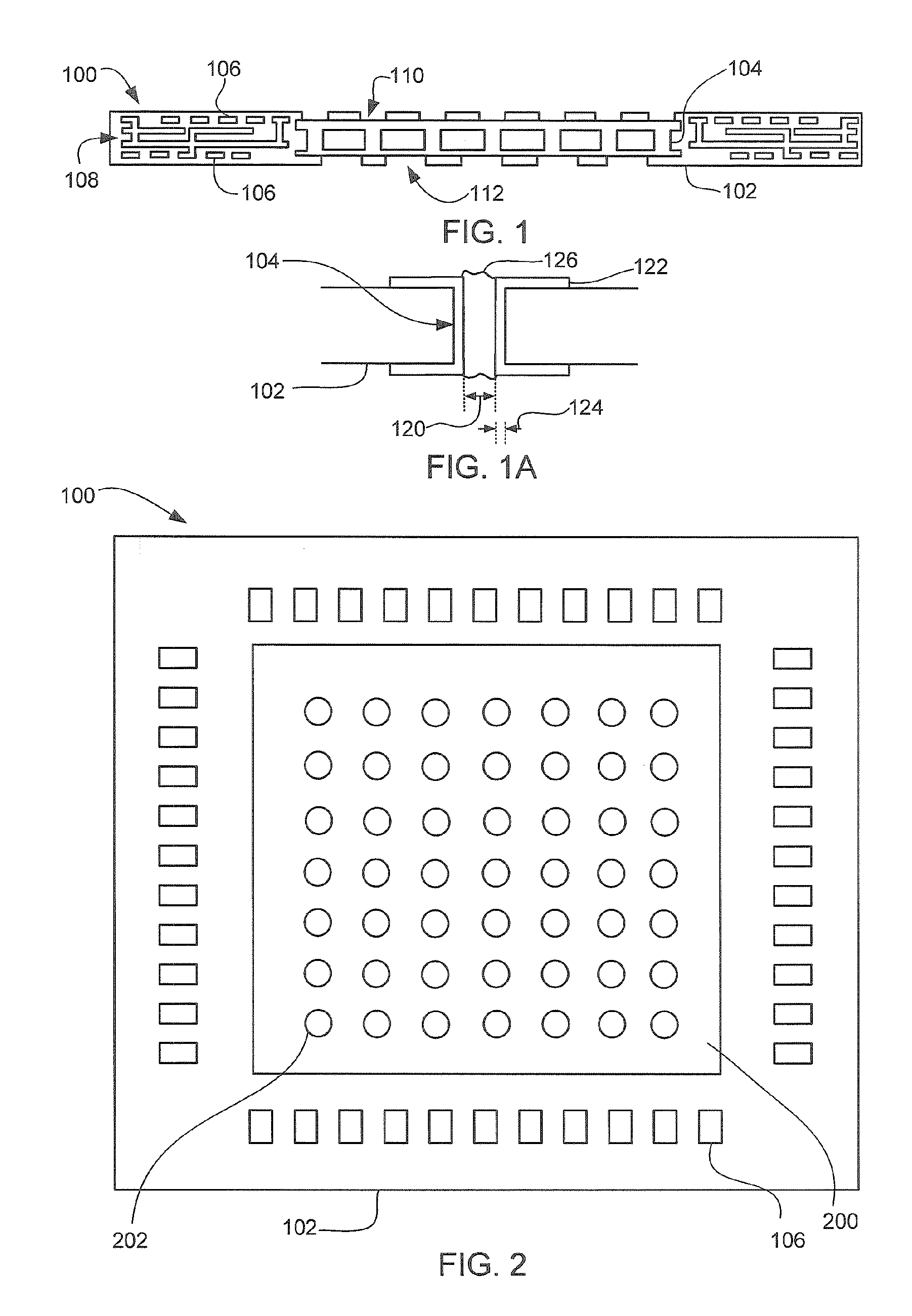
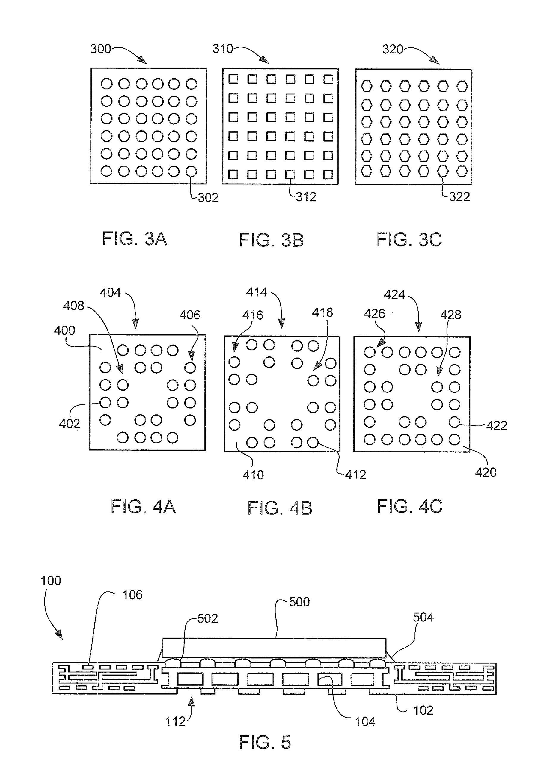
[0028]Likewise, the drawings showing embodiments of the device are semi-diagrammatic and not to scale and, particularly, some of the dimensions are for the clarity of presentation and are shown greatly exaggerated in the FIGs. In addition, where multiple embodiments are disclosed and described having some features in common, for clarity and ease of illustration and description thereof like features one to another will ordinarily be described with like reference numerals.

[0029]The term “horizontal” as used herein is defined as a plane parallel to the conventional plane or surface of the substrate, regardless of its orient...


PUM


Abstract

A semiconductor package system includes providing a substrate having a plurality of thermal vias extending through the substrate. A solder mask is positioned over the plurality of thermal vias. A plurality of thermally conductive bumps is formed on at least some of the plurality of thermal vias using the solder mask. An integrated circuit die is attached to the plurality of thermally conductive bumps. An encapsulant encapsulates the integrated circuit die.

Description

CROSS-REFERENCE TO RELATED APPLICATION(S)[0001]This application claims the benefit of U.S. Provisional Patent Application Ser. No. 60 / 593,858 filed Feb. 18, 2005, and the subject matter thereof is hereby incorporated herein by reference thereto.TECHNICAL FIELD[0002]The present invention relates generally to semiconductor package systems, and more particularly to a semiconductor package system providing enhanced thermal conductivity.BACKGROUND ART[0003]In the electronics industry, the continuing goal has been to reduce the size of electronic devices such as camcorders and portable telephones while increasing performance and speed. Integrated circuit packages for complex systems typically are comprised of a multiplicity of interconnected integrated circuit chips. The integrated circuit chips usually are made from a semiconductor material such as silicon or gallium arsenide. Semiconductor devices are formed in the various layers of the integrated circuit chips using photolithographic t...

Claims


Application Information

Patent Timeline
Patent Type & Authority Patents(United States)
IPC IPC(8): H01L23/12
CPCH01L23/3128H01L23/3677H01L23/4334H01L23/49816H01L24/83H01L2224/48091H01L2224/73265H01L2224/8314H01L2924/1815H01L2924/01029H01L2924/01322H01L24/48H01L2924/19105H01L2924/19041H01L2924/15311H01L2924/14H01L2224/92247H01L2224/85051H01L2224/83801H01L2224/48475H01L23/49838H01L24/85H01L2224/32225H01L2224/48227H01L2924/00012H01L2924/00014H01L2924/00H01L24/73H01L2924/181H01L2224/45099H01L2224/45015H01L2924/207
Inventor LEE, SANGKWONLEE, TAE KEUN
Owner STATS CHIPPAC LTD
Features
  • R&D
  • Intellectual Property
  • Life Sciences
  • Materials
  • Tech Scout
  • Unparalleled Data Quality
  • Higher Quality Content
  • 60% Fewer Hallucinations
Learn More