Dynamic tool scheduling based upon defects

a tool scheduling and defect technology, applied in the field of dynamic tool scheduling based on defects, can solve the problems of inability to timely occur, inability to efficiently and accurately process, and inability to provide processing tools without tedious manual intervention

Inactive Publication Date: 2010-05-18
ADVANCED MICRO DEVICES INC
View PDF12 Cites 13 Cited by
  • Summary
  • Abstract
  • Description
  • Claims
  • Application Information

AI Technical Summary

Benefits of technology

[0013]In one aspect of the present invention, a method is provided for routing a semiconductor wafer to at least one of a plurality of processing tools based upon tool performance. Data relating to a performance of a first processing tool and a performance of a second processing tool is acquired. A semiconductor wafer is routed to one of the first processing tool or the second processing tool based upon a comparison between the performance of the first processing tool and the performance of the second processing tool using a controller.
[0014]In another aspect of the present invention, a system is provided for routing a semiconductor wafer to at least one of a plurality of processing tools based upon performance. The system of the present invention comprises: a plurality of processing tools to process semiconductor wafers; and a process controller operatively coupled to the processing tools, the process controller to control operations of the processing tools and perform a selective tool-scheduling process, the selective tool-scheduling process comprising determining a hierarchy for a plurality of the processing tools based upon performance of the processing tools and routing a semiconductor wafer to at least one of the processing tools for processing based upon the hierarchy.
[0015]In another aspect of the present invention, an ap

Problems solved by technology

Utilizing current manufacturing methods, efficient matching of a particular process to the best available processing tool may not occur without tedious manual intervention.
Furthermore, isolation and/or tagging of particular processing tools that may be lagging behind other processing tools, in terms of efficiency and accuracy of processing, may not timely occur.
Among the problems associated with implementing the current proc

Method used


Image

  • Dynamic tool scheduling based upon defects
  • Dynamic tool scheduling based upon defects
  • Dynamic tool scheduling based upon defects

Examples


Embodiment Construction

[0027]Illustrative embodiments of the invention are described below. In the interest of clarity, not all features of an actual implementation are described in this specification. It will of course be appreciated that in the development of any such actual embodiment, numerous implementation-specific decisions must be made to achieve the developers' specific goals, such as compliance with system-related and business-related constraints, which will vary from one implementation to another. Moreover, it will be appreciated that such a development effort might be complex and time-consuming, but would nevertheless be a routine undertaking for those of ordinary skill in the art having the benefit of this disclosure.

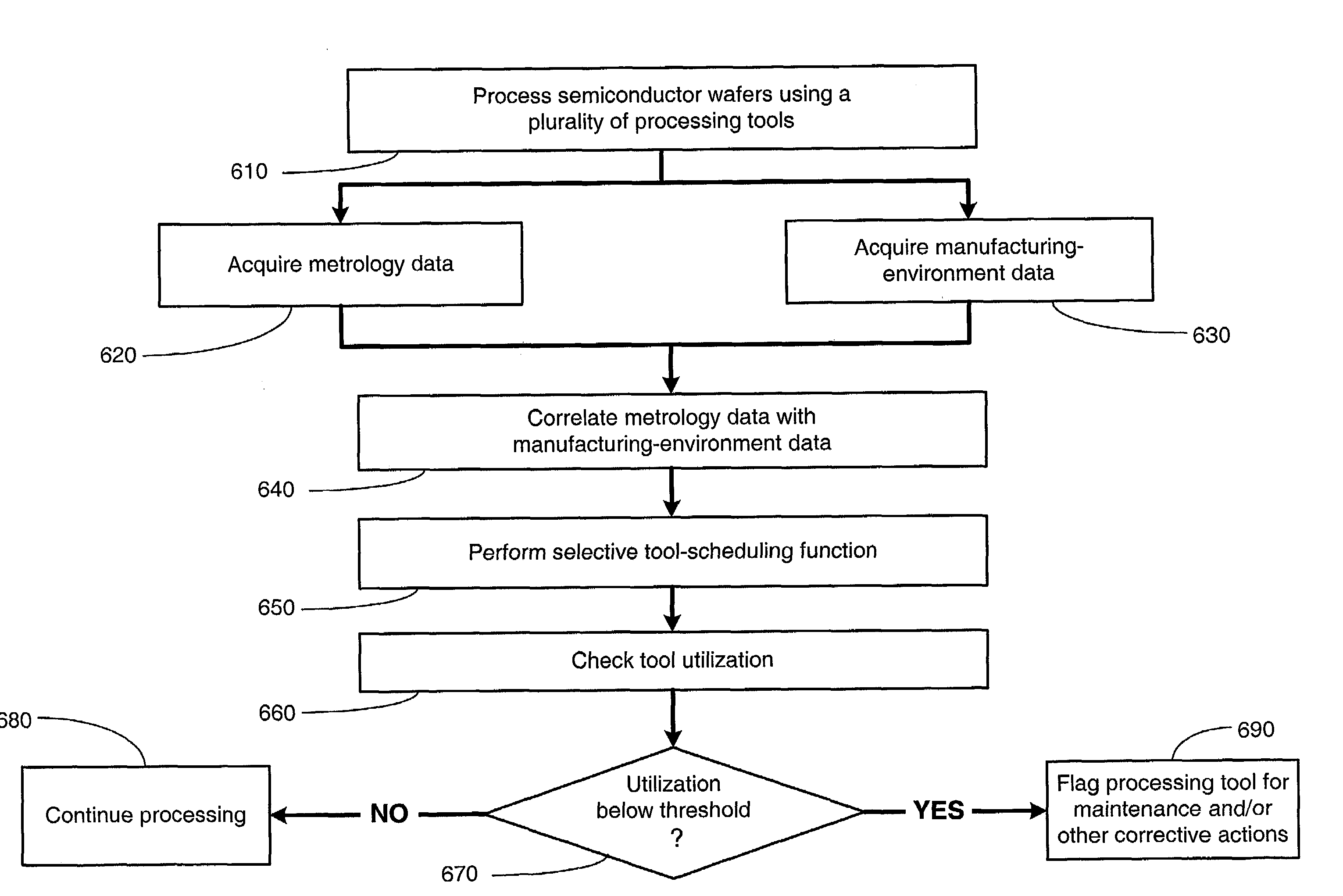
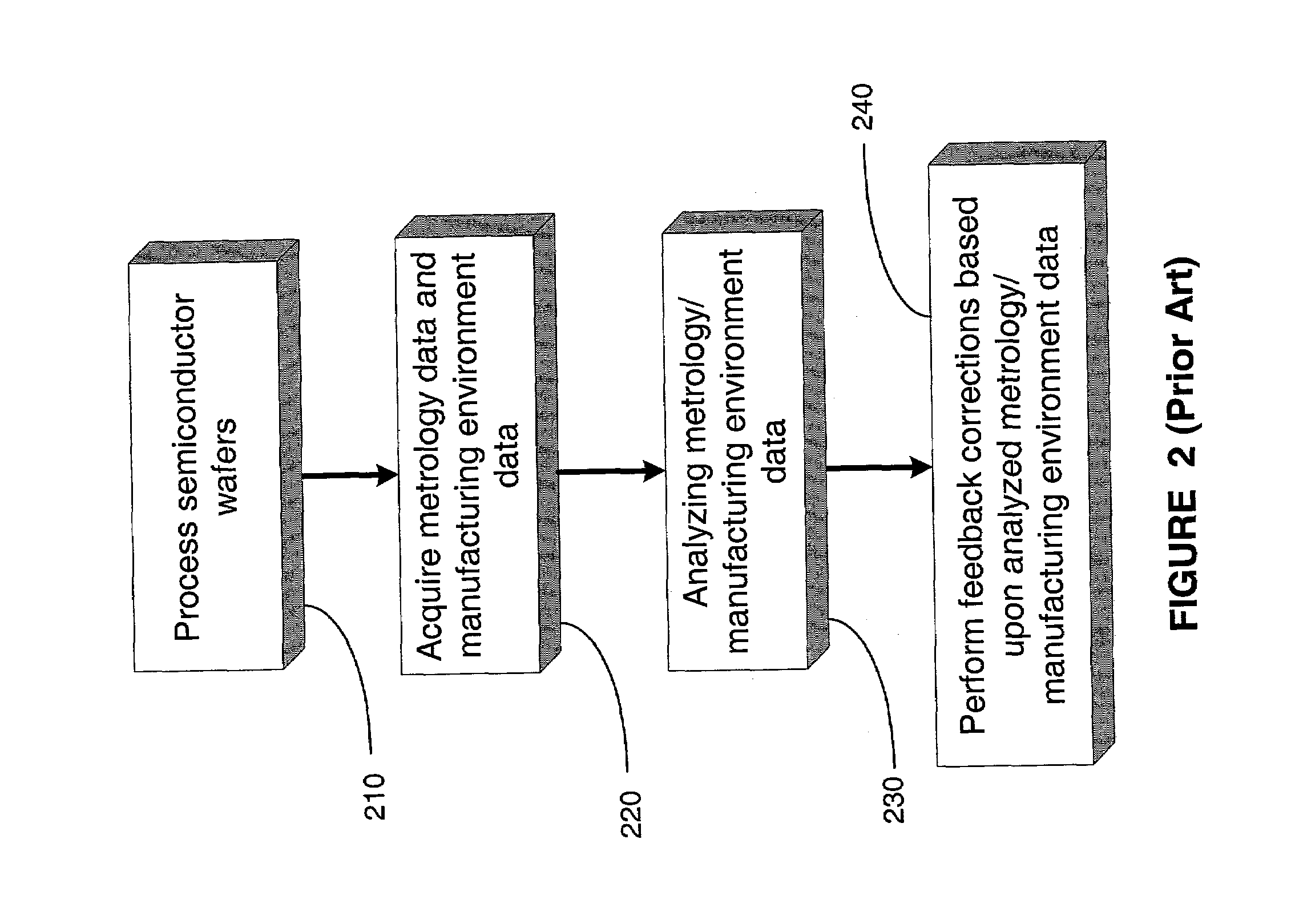
[0028]There are many discrete processes that are involved in semiconductor manufacturing. Many times, semiconductor devices are stepped through multiple manufacturing process tools. Scheduling a process flow that substantially matches particular processes with the best available ...


PUM


Abstract

A method and an apparatus for routing a semiconductor wafer to at least one of a plurality of processing tools based upon tool performance. Data relating to a performance of a first processing tool and a performance of a second processing tool is acquired. A semiconductor wafer is routed to one of the first processing tool or the second processing tool based upon a comparison between the performance of the first processing tool and the performance of the second processing tool using a controller.

Description

BACKGROUND OF THE INVENTION[0001]1. Field of the Invention[0002]This invention relates generally to semiconductor manufacturing, and, more particularly, to a method and apparatus for performing a tool scheduling process, which includes matching a particular process with an appropriate tool.[0003]2. Description of the Related Art[0004]The technology explosion in the manufacturing industry has resulted in many new and innovative manufacturing processes. Today's manufacturing processes, particularly semiconductor manufacturing processes, call for a large number of important steps. These process steps are usually vital, and therefore, require a number of inputs that are generally fine-tuned to maintain proper manufacturing control.[0005]The manufacture of semiconductor devices requires a number of discrete process steps to create a packaged semiconductor device from raw semiconductor material. The various processes, from the initial growth of the semiconductor material, the slicing of t...

Claims


Application Information

Patent Timeline
IPC IPC(8): G06F19/00
CPCG05B19/4187Y02P90/02
Inventor STEWART, EDWARD C.
Owner ADVANCED MICRO DEVICES INC
Why Eureka
Try Eureka