Communication timing changing method and device
a technology of communication timing and changing method, which is applied in the direction of generating/distributing signals, color television with bandwidth reduction, television systems, etc., can solve the problems of difficult to make the communication of control parameters with respective analog devices, and high power consumption of cpu, so as to prevent bad influence, increase the operating speed of cpu, and increase the power consumption and cost of cpu
- Summary
- Abstract
- Description
- Claims
- Application Information
AI Technical Summary
Benefits of technology
Problems solved by technology
Method used
Image


Examples
embodiment 1
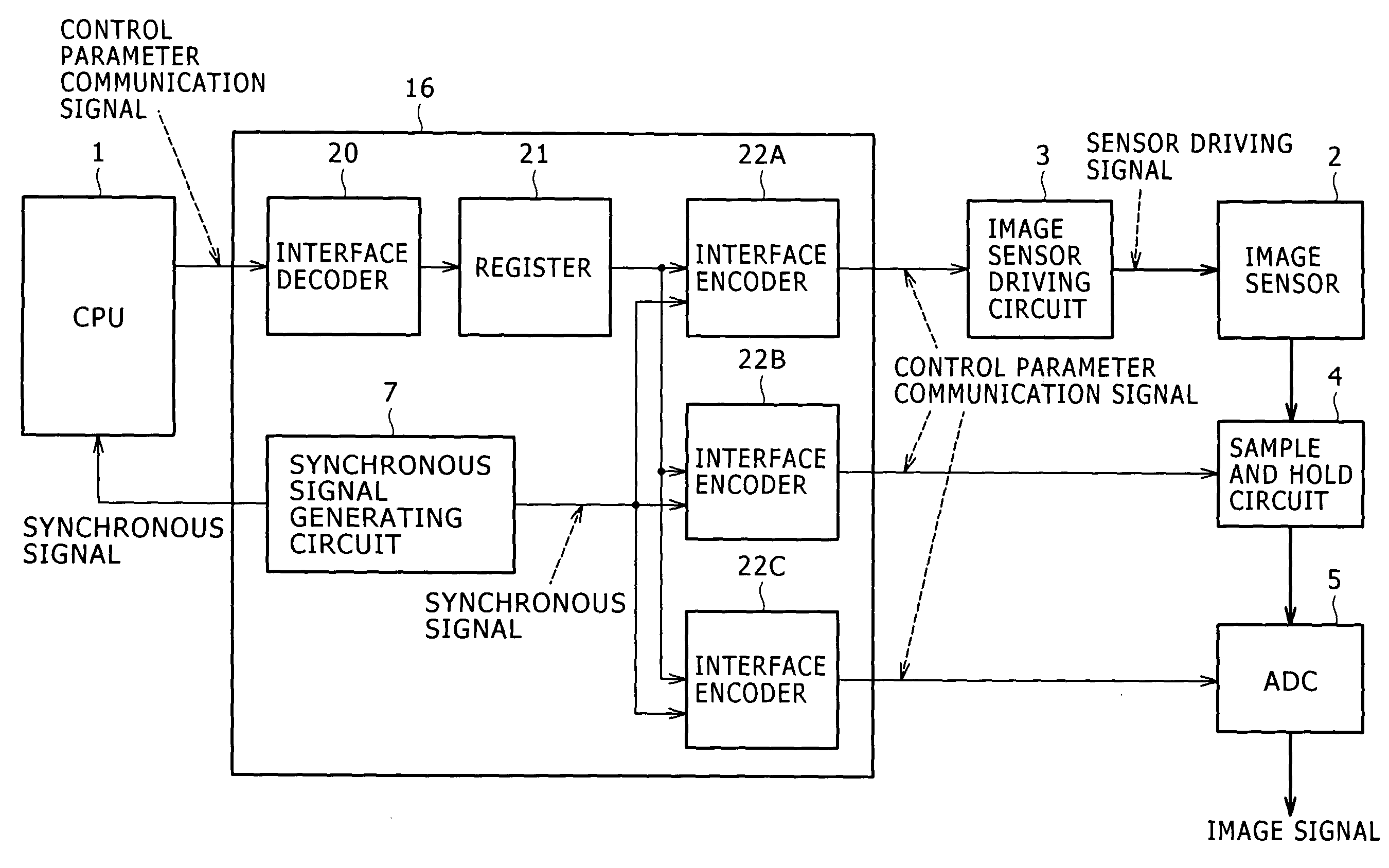
[0029]FIG. 1 is a block diagram showing a configuration of an image pickup device to which a communication timing changing method according to an embodiment 1 of the present invention is applied. The block diagram of FIG. 1 shows analog devices including an image sensor within the image pickup device, a CPU, and an integrated circuit interposed between the analog devices and the CPU. The timing of communication of control parameters made from the CPU to the analog devices is changed over to another one which does not impede any of operations of the analog devices through the integrated circuit, and control parameters are set in the analog devices, respectively.
[0030]The image pickup device includes an image sensor 2, an image sensor driving circuit 3, a sample and hold circuit 4, and an analog / digital converter (hereinafter referred to as “an ADC”) 5 as analog devices.
[0031]An integrated circuit 16 is interposed between the CPU 1 and the analog devices. The CPU 1 can control all of ...
embodiment 2
[0050]FIG. 3 is a block diagram showing a configuration of an image pickup device to which a communication timing changing method according to an embodiment 2 of the present invention is applied. In FIG. 3, portions identical or corresponding to those shown in FIG. 1 are designated with the same reference numerals, and a description thereof is omitted here. A point of difference of the embodiment 2 from the embodiment 1 described above is that in the embodiment 1 described above, the interface encoders 22A, 22B and 22C are provided so as to correspond to the image sensor driving circuit 3, the sample and hold circuit 4, and the ADC 5 as the analog devices, respectively, whereas in the embodiment 2, only the interface encoder (a communication section) 22D communicates with all the analog devices. In addition, an integrated circuit (an electronic device) 26 includes the synchronous signal generating circuit 7, the interface decoder 20, the register 21 and the interface encoder 22D.
[00...
embodiment 3
[0056]FIG. 5 is a block diagram showing a configuration of an image pickup device to which a communication timing changing method according to an embodiment 3 of the present invention is applied. In FIG. 5, portions identical or corresponding to those shown in FIG. 3 are designated with the same reference numerals, and a description thereof is omitted here. A point of difference of the embodiment 3 from the embodiment 1 described above is that in the embodiment 1, the integrated circuit 16 and the CPU 1 are formed on the different chips, respectively, whereas in the embodiment 3, the CPU 1 is formed on the same chip as that of the synchronous signal generating circuit 7, the register 21, and the interface encoder 22D, and thus incorporated in an integrated circuit (electronic device) 36.
[0057]According to the embodiment 3, incorporating the CPU 1 in the integrated circuit 36 results in that the CPU 1 can directly write the control parameters to the register 21. Hence, there is offer...
PUM
 Abstract
Description
Claims
Application Information