High sensitivity sensor device and manufacturing thereof

a sensor device and high sensitivity technology, applied in the direction of instruments, chemical methods analysis, analysis using chemical indicators, etc., can solve the problem that the guided light usually suffers radiation loss, and achieve the effect of reducing the output optical power

Active Publication Date: 2011-04-12
BANPIL PHOTONICS
View PDF3 Cites 21 Cited by
  • Summary
  • Abstract
  • Description
  • Claims
  • Application Information

AI Technical Summary

Benefits of technology

[0011]This sensor detects the concentration of gases (that exist in air) based on the change in the effective refractive index of the substrate caused when biomolecule gas / chemical agents fill the air (or receptor) spaces. The changes in the effective refractive index reduce the output optical power (measurable parameter). By comparing the output optical power with the reference input optical power, the proposed nanosensor can detect the biomolecule gas, / chemical agent concentration in ppb levels.

Problems solved by technology

In waveguide, the guided light usually suffers radiation loss due to weak optical confinement; this happens when the structure is not well optimized or the structural parameters are interrupted.

Method used


Image

  • High sensitivity sensor device and manufacturing thereof
  • High sensitivity sensor device and manufacturing thereof
  • High sensitivity sensor device and manufacturing thereof

Examples


Embodiment Construction

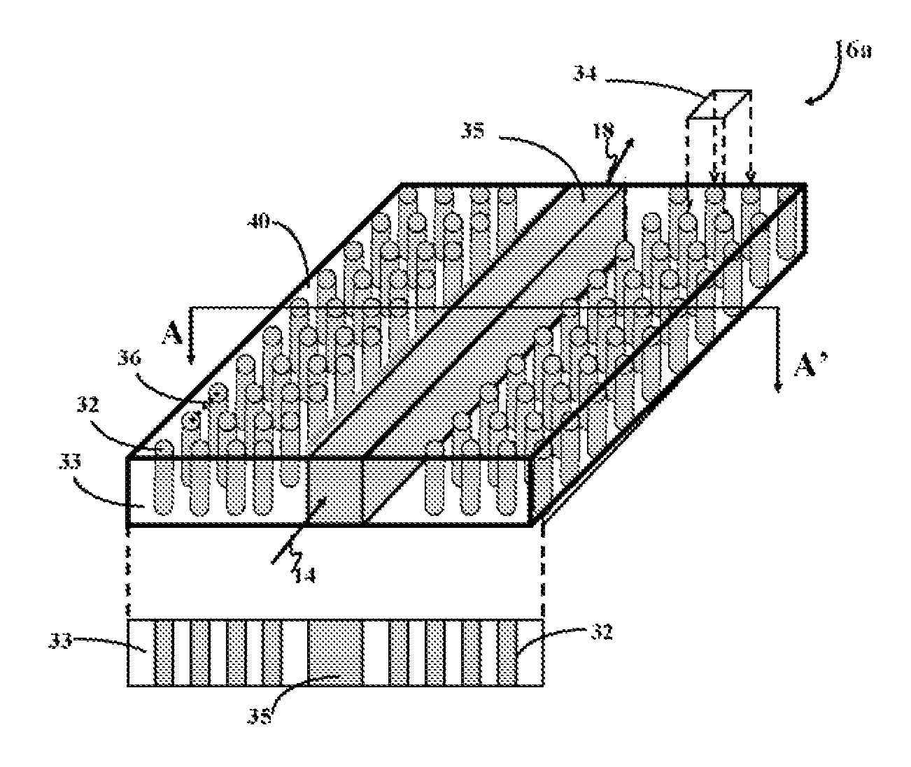
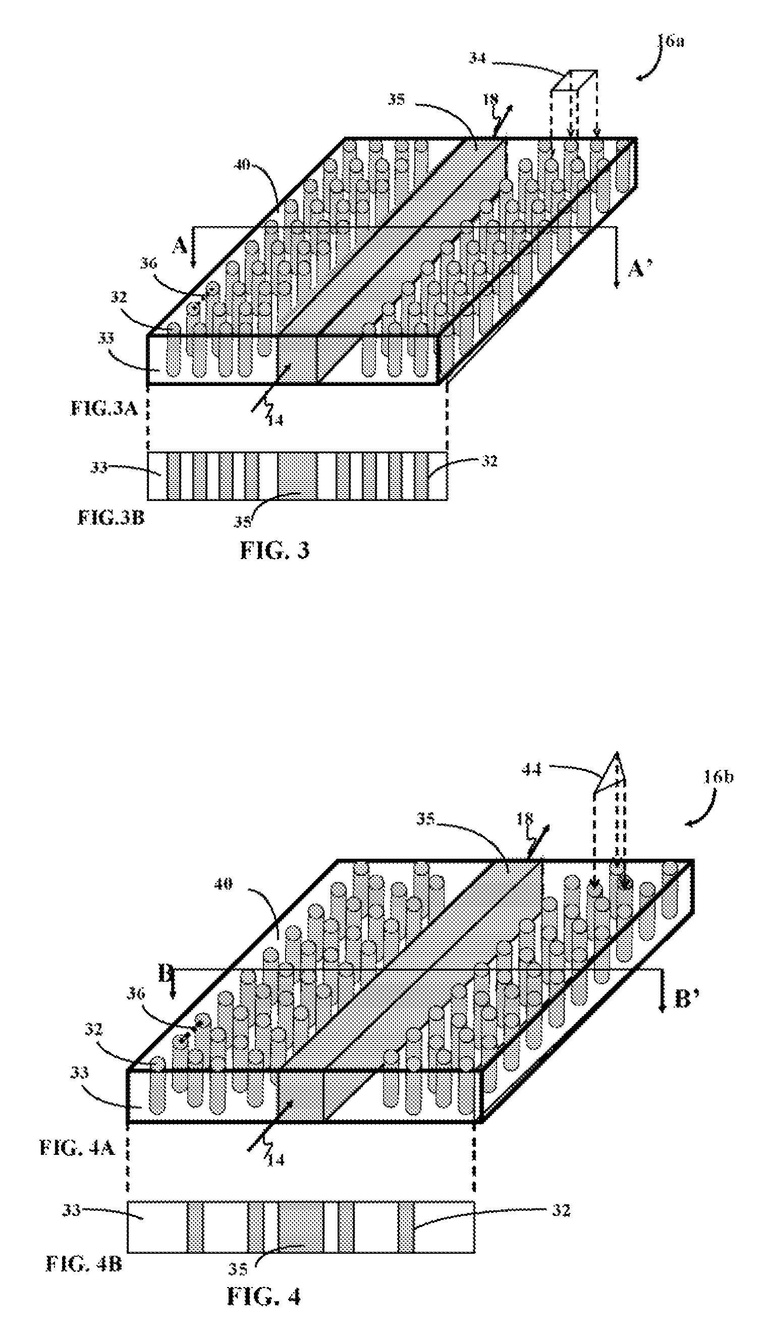
[0032]In the following detailed description of the preferred embodiments, reference is made to the accompanying drawings, which form a part hereof and in which is shown by way of illustration specific preferred embodiments in which the inventions may be practiced. These embodiments are described in sufficient detail to enable those skilled in the art to practice the invention and it is to be understood that other embodiments may be utilized. The following detailed description is, therefore, not to be taken in a limiting sense, and the scope of the present invention is defined only by the appended claims.

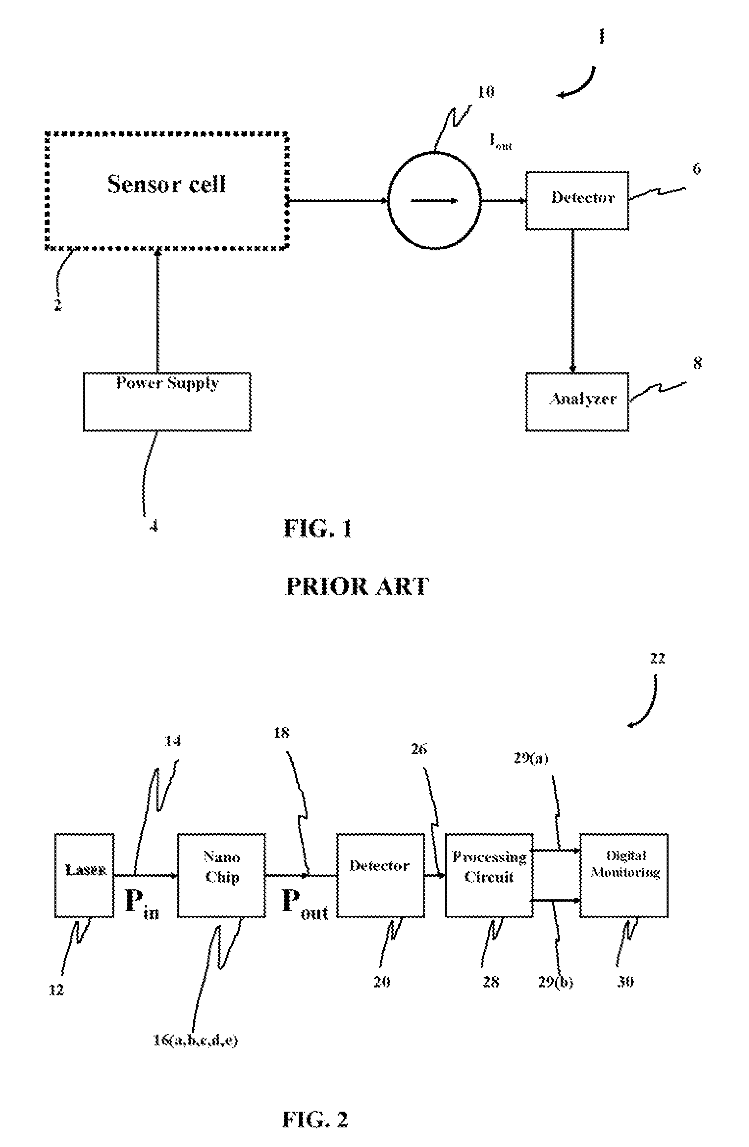
[0033]According to this current invention, it is our objective to provide a sensing device comprising with nanosensor and its signal processing circuit which can have the significantly high sensitivity. The sensor device detects the specimen concentration based on the principle of optics Using of the nano-sensor and signal processing circuit, according to this invention, high sensiti...


PUM

PropertyMeasurementUnit
quantum efficiencyaaaaaaaaaa
refractive indexaaaaaaaaaa
timeaaaaaaaaaa

Abstract

A sensing device able to do concurrent real time detection of different kinds of chemical, biomolecule agents, or biological cells and their respective concentrations using optical principles. The sensing system can be produced at a low cost (below $1.00) and in a small size (˜1 cm3). The novel sensing system may be of great value to many industries, for example, medical, forensics, and military. The fundamental principles of this novel invention may be implemented in many variations and combinations of techniques.

Description

FIELD OF THE INVENTION[0001]The present invention relates to high sensitivity sensor devices and its related signal processing circuits to detect the gas, biomolecules, or biochemical agents. More specifically, this invention is related to sensor device comprising with at least one nano-chip for application in biomedical and industrial applications.BACKGROUND OF THE INVENTION[0002]A large benefit of this sensor according to this invention, is that there can be several on a single wafer. It is a device able to measure chemical agent concentrations at the part-per-billion (ppb) level and accurately determine the biomolecule agent and volume of biological cells present in human body. There is no device in the state-of-art, which allows concurrent detection of a chemical agent, biomolecule agent, and biological cell, all in a single system.[0003]There are various kinds of sensor system. FIG. 1 shows a schematic representing the prior art of a sensor system 1 to detect biological cells, ...

Claims


Application Information

Patent Timeline
Patent Type & Authority Patents(United States)
IPC IPC(8): G01N21/00
CPCB82Y20/00G02B6/1225G01N21/7703G02B2006/12138
Inventor DUTTA, ACHYUT KUMARSENGUPTA, RABI S
Owner BANPIL PHOTONICS
Why Eureka
Try Eureka