

Semiconductor heterostructure
a technology of semiconductors and heterostructures, applied in the field of semiconductor heterostructures, can solve the problems of increasing the capture time , reducing the capture efficiency of devices, and less effective coupling with localized states inside narrow bandgap layers, etc., and achieve the effect of enhancing the total light generation capability
- Summary
- Abstract
- Description
- Claims
- Application Information
AI Technical Summary
Benefits of technology
Problems solved by technology
Method used
Image

Examples
Embodiment Construction
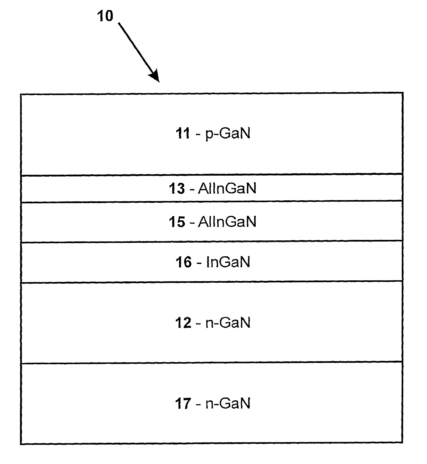
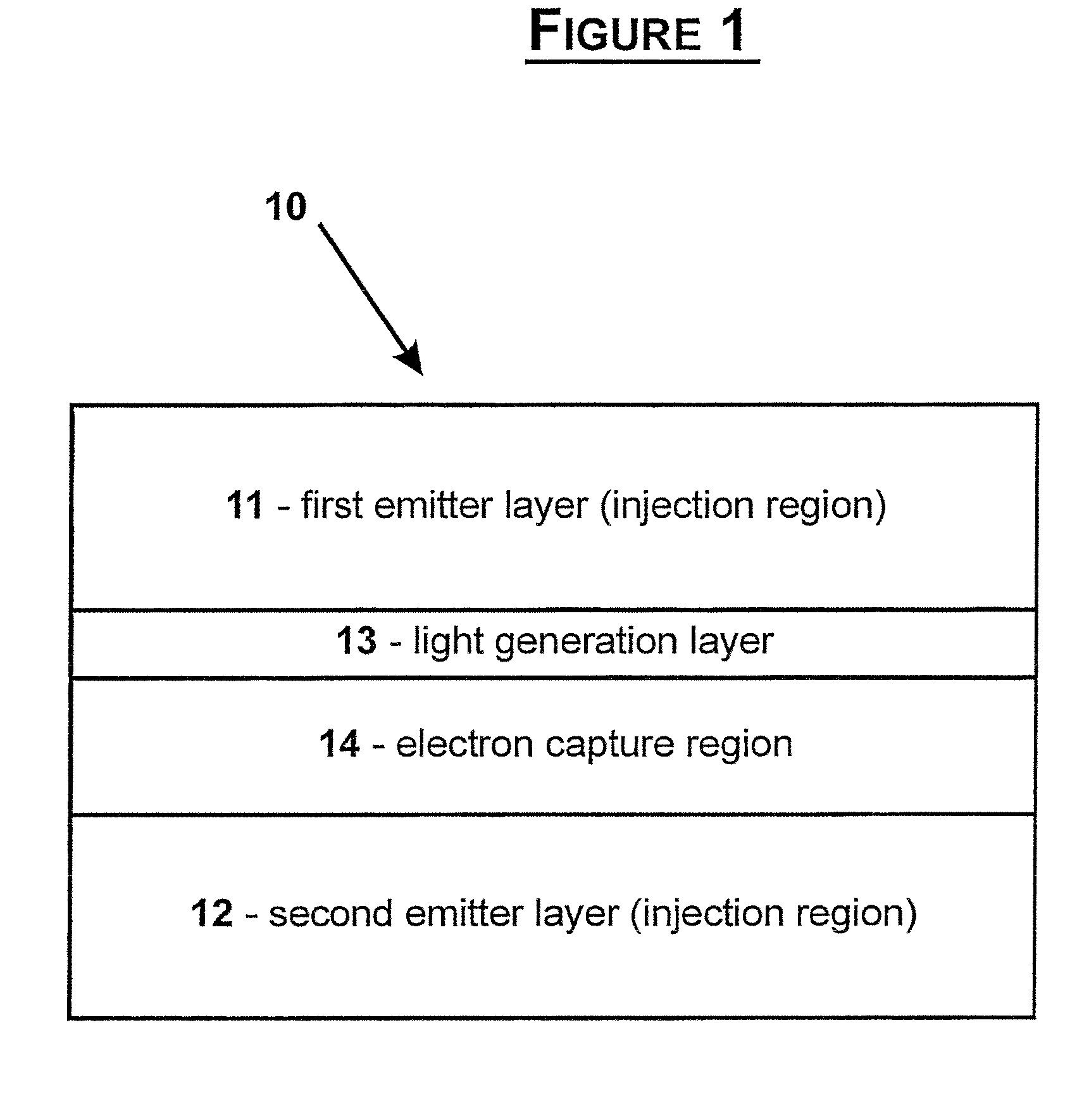
[0034]In FIG. 1 a cross-sectional schematic view of the semiconductor heterostructure is shown. The heterostructure, which is generally designated by 10, comprises an injection region consisting of a first emitter layer 11 and a second emitter layer 12, a light generation layer 13, and an electron capture region 14 consisting of a capture layer and a confining layer.
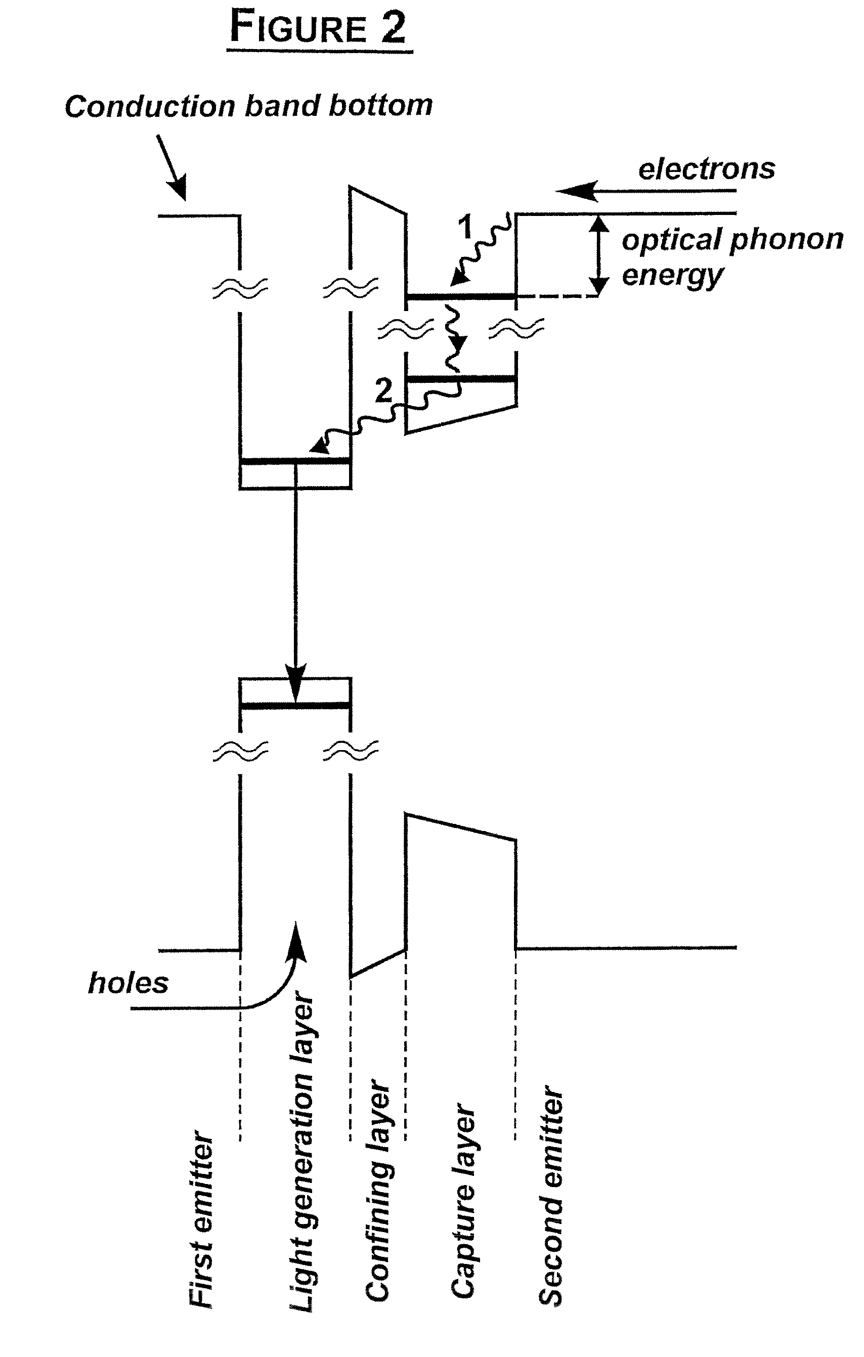
[0035]FIG. 2 represents a schematic energy band diagram of the heterostructure shown in FIG. 1. The capture region is a narrow bandgap layer adjacent to the second emitter layer. The layer with a wide bandgap between the capture and light generation layers is the confining layer. Widths and compositions of the capture and confining layers are adjusted to provide energy difference between one of the localized electron energy levels of the capture layer and the conduction band bottom in the electron emitter equal to the optical phonon energy. The capture of electrons into the narrow bandgap capture layer occurs due to inte...
PUM
 Abstract
Description
Claims
Application Information