Method for producing semiconductor components and thin-film semiconductor component
- Summary
- Abstract
- Description
- Claims
- Application Information
AI Technical Summary
Problems solved by technology
Method used
Image

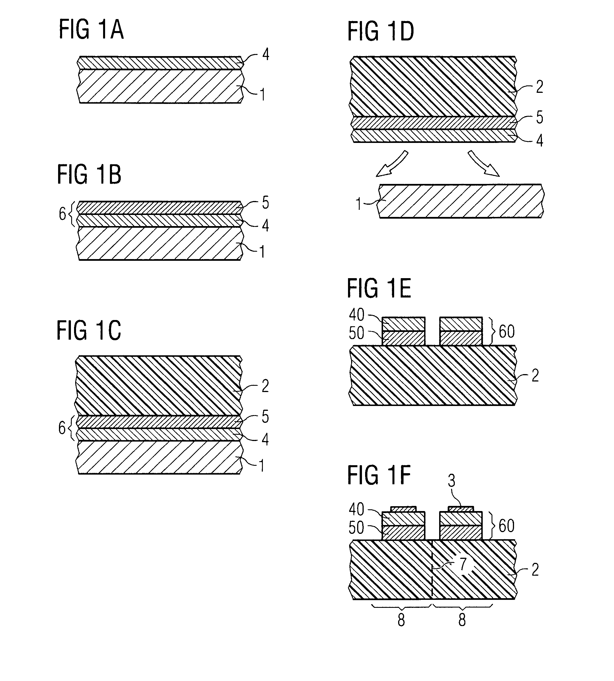
Examples
Example
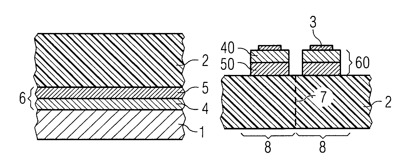
[0103]In accordance with a first embodiment, the semiconductor components 8 are present in singulated fashion, severed along the separating plane 7. They can be incorporated as individual semiconductor components for example in a housing body. Since the carrier layer is formed in a rigid, self-supporting and sufficiently stable manner, the semiconductor components 8 can be handled easily without the need for an additional auxiliary carrier for further processing.
[0104]Furthermore, the carrier layer 2 is preferably formed in electrically conductive fashion, such that the semiconductor component 8 can be connected to a first electrode on the rear side via the carrier layer 2. The semiconductor component 8 can be connected to a second electrode on the top side via the second contact metallization 3. Furthermore, the contact metallization 50 is electrically conductive and reflects the radiation generated by the active layer stack 40. The radiation efficiency in the emission direction 9 ...
Example
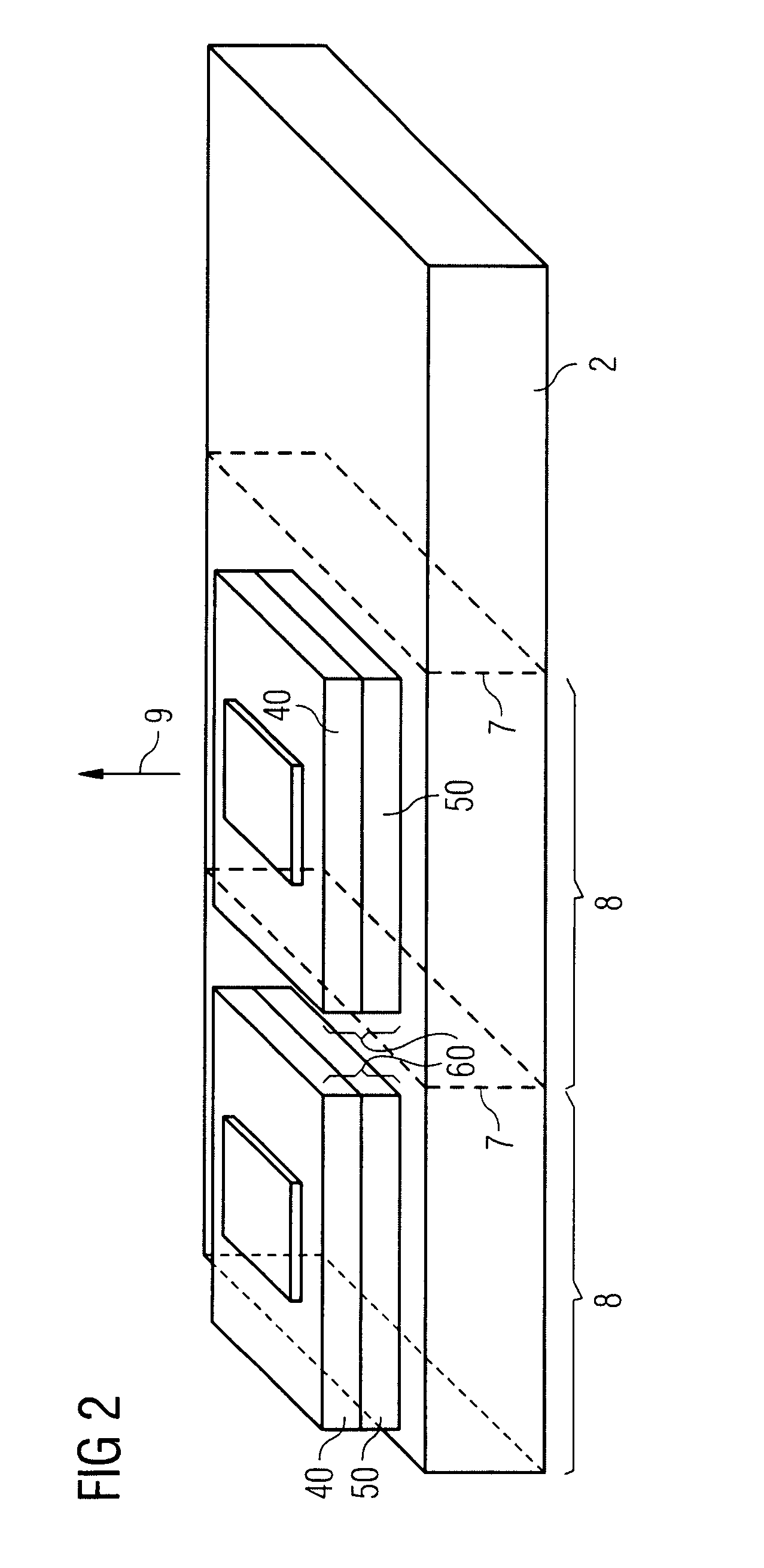
[0105]In accordance with a second embodiment, the carrier layer 2 is not severed. Rather, the layer stacks 60 arranged on the carrier layer 2 form a matrix. The carrier layer 2 can be electrically conductive, for example. As an alternative, the carrier layer 2 can be electrically insulating and have separately applied conductor tracks. Said conductor tracks can connect the layer stacks 60 to one another in any desired, predetermined manner.
[0106]A matrix arrangement of this type can be used for example for a display or a display backlighting.
[0107]FIG. 3 illustrates a semiconductor component 8 according to the invention which has the layer stack 60 arranged on the carrier layer 2, with the second contact metallization 3 applied on said layer stack.
[0108]In this exemplary embodiment, the contact metallization 50 is electrically conductive and transmissive to the radiation generated by the active layer stack 40. Furthermore, the carrier layer 2 is electrically insulating and transmiss...
PUM
 Abstract
Description
Claims
Application Information
 - Generate Ideas
- Intellectual Property
- Life Sciences
- Materials
- Tech Scout
- Unparalleled Data Quality
- Higher Quality Content
- 60% Fewer Hallucinations
Browse by: Latest US Patents, China's latest patents, Technical Efficacy Thesaurus, Application Domain, Technology Topic, Popular Technical Reports.
© 2025 PatSnap. All rights reserved.Legal|Privacy policy|Modern Slavery Act Transparency Statement|Sitemap|About US| Contact US: help@patsnap.com