
Fuse circuit and redundancy circuit
a fuse circuit and redundancy circuit technology, applied in the direction of digital storage, electrical equipment, instruments, etc., can solve the problems of ineffective disposal of semiconductor memory devices as defective products, inability to perform desired operations of semiconductor memory devices, and failure of a relatively small number of memory cells, so as to prevent the cracking of the fuse effect of semiconductor memory devices
- Summary
- Abstract
- Description
- Claims
- Application Information
AI Technical Summary
Benefits of technology
Problems solved by technology
Method used
Image

Examples
Embodiment Construction
[0060]Other objects and advantages of the present invention can be understood by the following description, and become apparent with reference to the embodiments of the present invention.
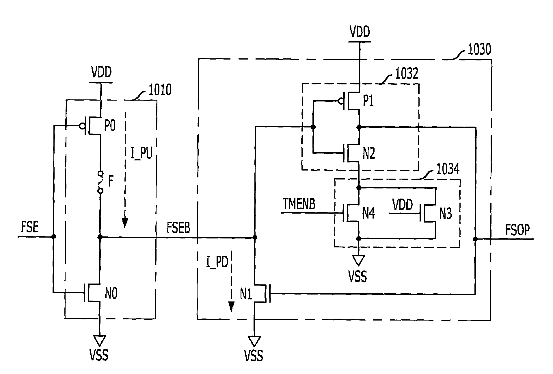
[0061]FIG. 10 illustrates a fuse circuit in accordance with an embodiment of the present invention.
[0062]Referring to FIG. 10, the fuse circuit includes a fuse block 1010 and a voltage detection block 1030.
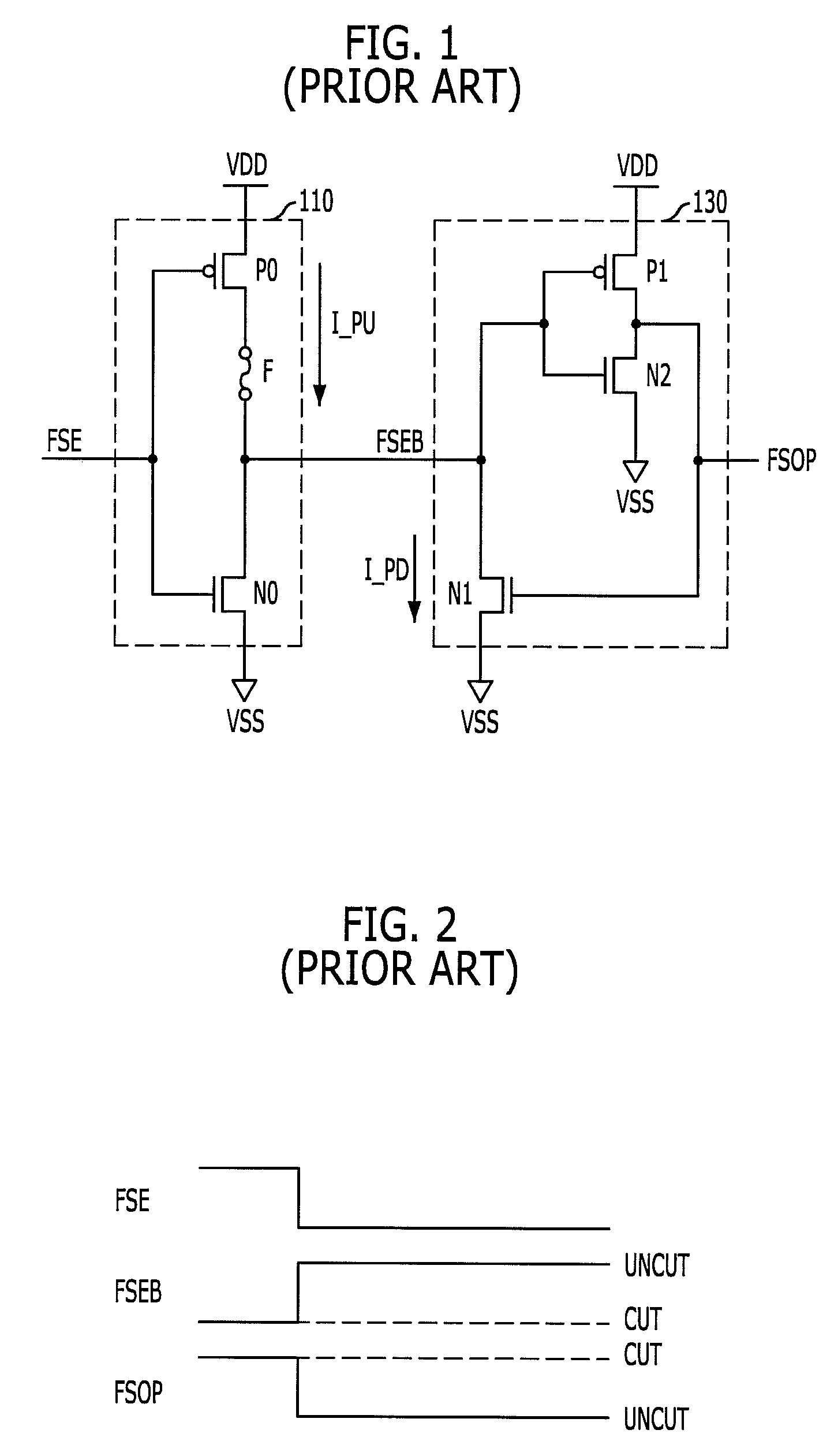
[0063]The fuse block 1010 includes a 0th PMOS transistor P0, a fuse F and a 0th NMOS transistor N0 that are connected in series between an external supply voltage (VDD) terminal and a ground voltage (VSS) terminal, wherein a fuse enable signal FSE is provided to gates of the 0th PMOS transistor P0 and the 0th NMOS transistor N0. Herein, the fuse enable signal FSE transfers from a logic high to a logic low if a power-up operation of a semiconductor memory device is terminated and thus internal and external reset operations are terminated. Thus, the fuse block 1010 can drive its output node through ...
PUM
 Abstract
Description
Claims
Application Information