High-speed contactor interconnect with circuitry

US8269516B1Active Publication Date: 2012-09-18XILINX INC

Image

  • High-speed contactor interconnect with circuitry
  • High-speed contactor interconnect with circuitry
  • High-speed contactor interconnect with circuitry

Examples


Embodiment Construction

[0015]In the following description, numerous specific details are set forth to provide a more thorough description of the specific embodiments of the invention. It should be apparent, however, to one skilled in the art, that the invention may be practiced without all the specific details given below. In other instances, well known features have not been described in detail so as not to obscure the invention. For ease of illustration, the same number labels are used in different diagrams to refer to the same items; however, in alternative embodiments the items may be different.

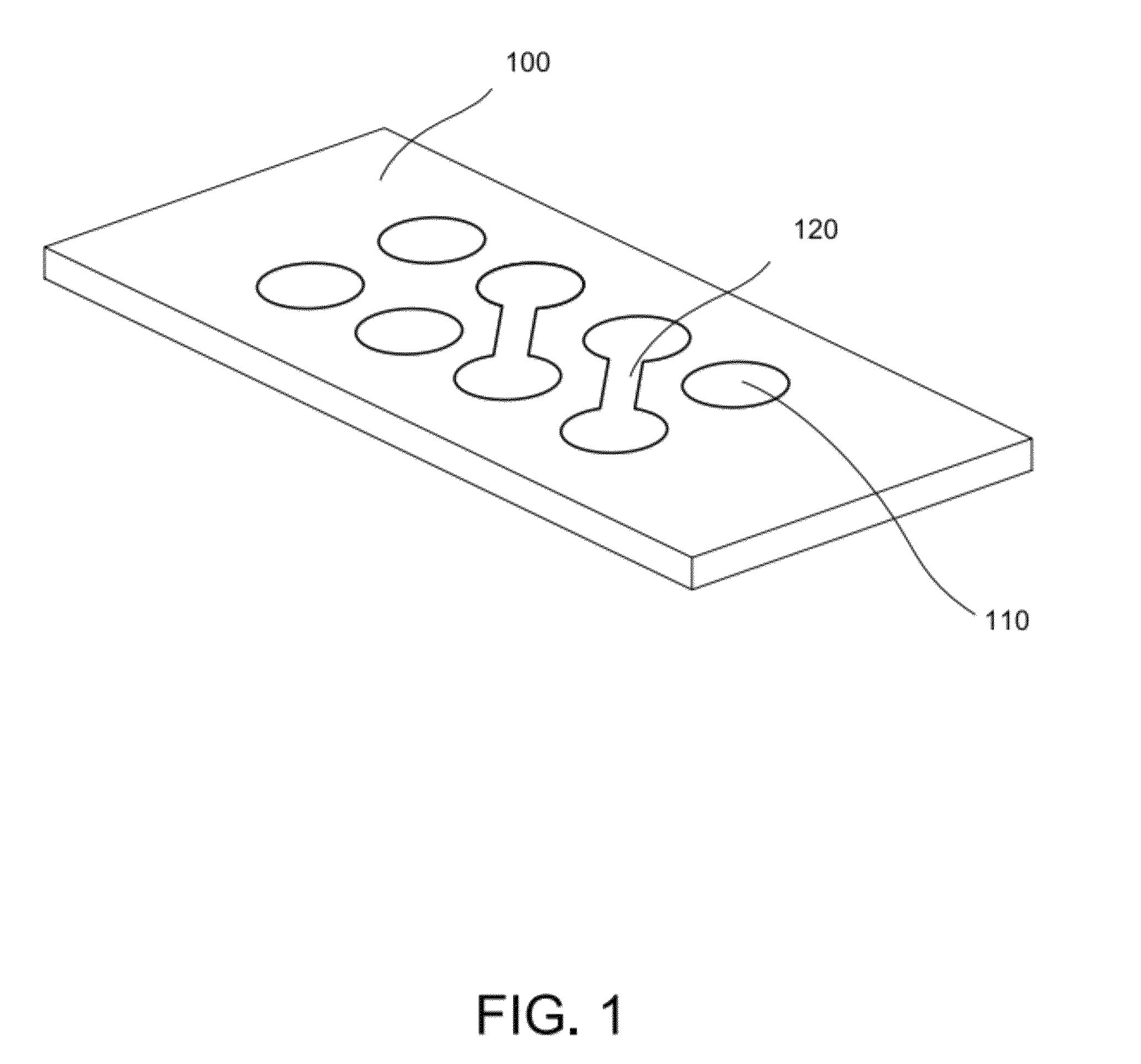
[0016]FIG. 1 illustrates a contact array in a test fixture with interconnected contact pads, in accordance with an embodiment of the present invention. In the embodiment illustrated, test fixture 100 is a plain rectangular shaped platform with a rectangular array of contact pads 110. Two pairs of contact pads 110 are interconnected 120 at the contacting surface of the test fixture.

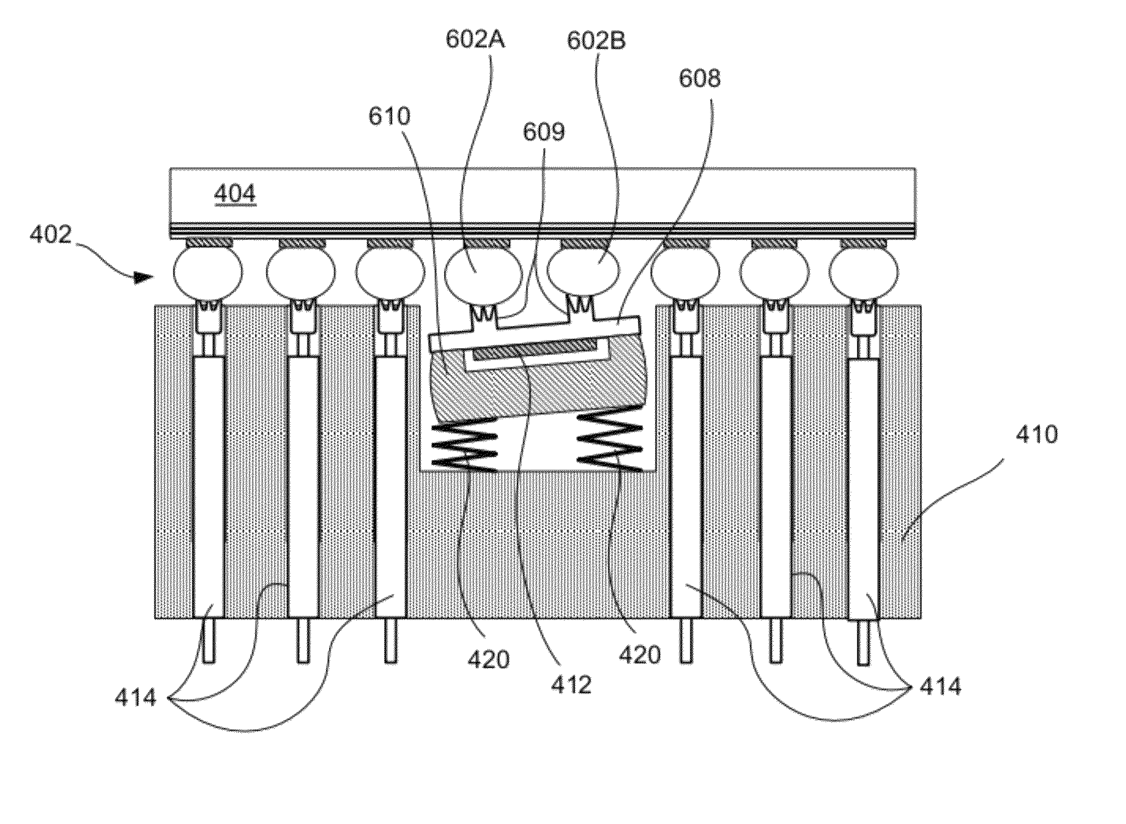
[0017]It is noted here that th...


PUM


Abstract

Disclosed is a contactor interconnect in an integrated circuit device test fixture comprises a plurality of contactor pins enabled to provide electrical contact with the contact points of an integrated circuit device, the contactor pins being mounted in the test fixture; and an electrical circuit coupled to two or more of the contactor pins of the test fixture, wherein the electrical circuit is isolated from other contactor pins of the plurality of contactor pins and wherein the electrical circuit is coupled to the two or more contactor pins by an electronically direct pathway.

Description

FIELD OF THE INVENTION[0001]The present application relates generally to integrated circuits, and in particular, to an integrated circuit testing apparatus and methods.BACKGROUND OF THE INVENTION[0002]Modern integrated circuit devices continue to shrink in size as they accelerate in speed. More and more functionality is demanded of less and less device “real estate” or available circuit space, whether on the printed circuit board of an electronic appliance or on the semiconductor die in which integrated circuits are formed.[0003]One result of the shrinking of integrated circuits is the increasing density of the arrays of contacts that connect the circuit to the outside world. Typically formed of ball grid arrays (BGAs), a device's contacts can number in the thousands and be packed into an area of a few square centimeters.[0004]In a typical integrated circuit package, a package substrate provides connection between the BGA and a solder bump array[0005]Testing of a packaged integrated...

Claims


Application Information

Patent Timeline
18 Sep 2012
Publication
US8269516B1
IPC
G01R31/20
CPC
G01R1/06722
Inventors
MARDI, MOHSEN H.; MAHONEY, DAVID M.