Method and structure to reduce FET threshold voltage shift due to oxygen diffusion

a technology of oxygen diffusion and threshold voltage, applied in the field of methods, can solve the problems of shifting high contamination sensitivity of materials, and difficulty in reducing the switching threshold of the transistor, so as to reduce or avoid the contamination of hi-k dielectric materials

Inactive Publication Date: 2015-07-28
ALSEPHINA INNOVATIONS INC
View PDF11 Cites 4 Cited by
  • Summary
  • Abstract
  • Description
  • Claims
  • Application Information

AI Technical Summary

Benefits of technology

[0005]It is therefore an object of the present invention to provide a method and structure that reduces or avoids contamination of Hi-K dielectric materials by diffused oxygen in integrated circuits.
[0006]It is another object of the present invention to provide high-performance, aggressively scaled field effect transistors in integrated circuits that do not exhibit significant shift in threshold voltage.

Problems solved by technology

However, such materials have a high sensitivity to contamination, particularly by oxygen.
Contamination of Hi-K materials by oxygen is particularly problematic since oxygen contamination, in which oxygen diffuses into vacancies in the Hi-K material, alters the work function of the gate and causes a shift in the switching threshold of the transistor.
Unfortunately, many commonly required structures in integrated circuits, such as insulators or isolation structures are formed of oxides or otherwise provide a source of oxygen that can contaminate Hi-K materials during manufacture and / or operation due to thermal diffusion.
Of particular concern is the fact that thermal diffusion of oxygen can continue after an integrated circuit is placed in service and degrade performance beyond specifications that were originally met.

Method used


Image

  • Method and structure to reduce FET threshold voltage shift due to oxygen diffusion
  • Method and structure to reduce FET threshold voltage shift due to oxygen diffusion
  • Method and structure to reduce FET threshold voltage shift due to oxygen diffusion

Examples


Embodiment Construction

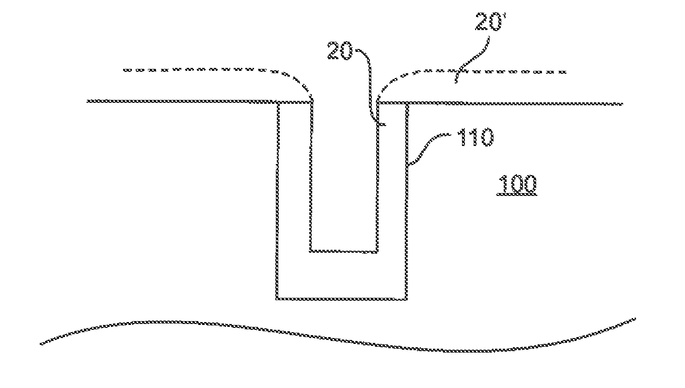
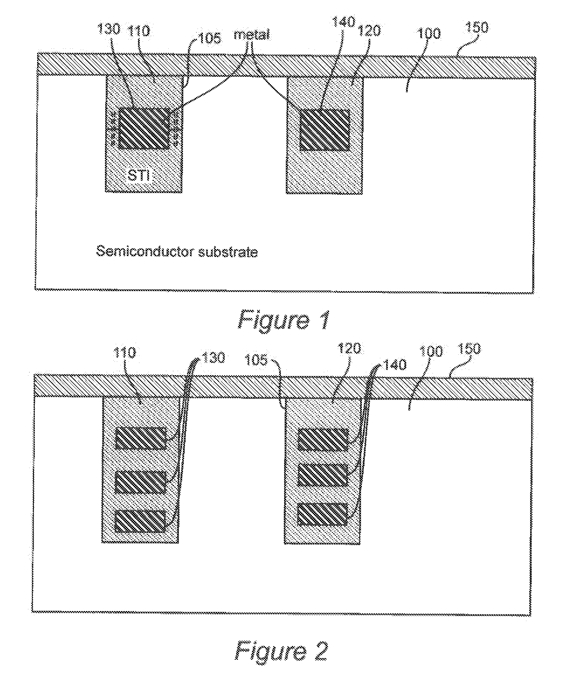
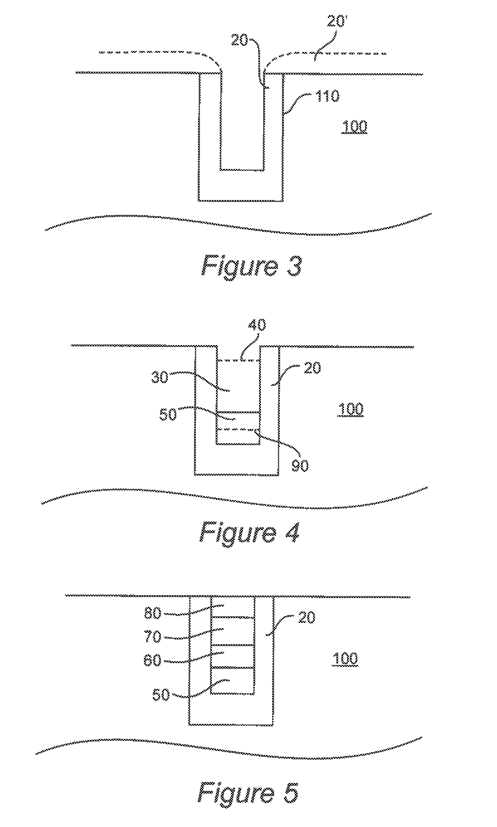
[0014]Referring now to the drawings, and more particularly to FIG. 1, there is shown in a cross-sectional view of a representative portion of a semiconductor substrate 100 including a first exemplary embodiment of the invention. As will be recognized by those skilled in the art of semiconductor integrated circuit manufacture, the structure illustrated in cross-section in FIG. 1 represents a very early stage in the manufacture of a given integrated circuit design since the only structures produced on the substrate are shallow trench isolation (STI) structures 110 and 120 for electrical and physical separation of electronic elements such as transistors which will be formed between them during a so-called front end of line (FEOL) stage of manufacture. Therefore, the position, pattern and density of formation of such STI structures will essentially outline the areas where such active and other devices will be formed on the chip.

[0015]It also follows that the pattern and density of such ...


PUM


Abstract

Oxygen scavenging material embedded in an isolation structure provides improved protection of high dielectric constant (Hi-K) materials from oxygen contamination while avoiding alteration of work function and switching threshold shift in transistors including such Hi-K materials.

Description

FIELD OF THE INVENTION[0001]The present invention generally relates to integrated circuits including field effect transistors and, more particularly, to avoiding contamination of high dielectric constant (Hi-K) gate insulator structures therein.BACKGROUND OF THE INVENTION[0002]Demand for increased functionality and performance of integrated circuits has driven designs to extremely high integration density of electronic elements therein that are scaled to extremely small feature sizes. High integration density allows more electronic elements to be provided on a semiconductor chip of a given size while small size and close proximity of those electronic elements reduces signal propagation time, allowing higher clock speeds, and noise susceptibility. Many sophisticated structures have been designed and exotic materials employed to maintain adequate electrical operating margins for transistors and field effect transistors, in particular, as transistors have been scaled to such extremely ...

Claims


Application Information

Patent Timeline
Patent Type & Authority Patents(United States)
IPC IPC(8): H01L21/02H01L29/66H01L21/762H01L29/78
CPCH01L21/76224H01L21/762H01L29/66537H01L29/783H01L29/0649
Inventor BAIOCCO, CHRISTOPHER VINCENTCHUDZIK, MICHAEL P.NAIR, DELEEP R.SHAH, JAY M.
Owner ALSEPHINA INNOVATIONS INC
Why Eureka
Try Eureka