Capacitive sensing array device with high sensitivity and electronic apparatus using the same

a sensing array and high sensitivity technology, applied in the direction of resistance/reactance/impedence, instruments, pulse techniques, etc., can solve the problems of large sensing error, high cost, and decrease in sensitivity, and achieve high sensitivity and high sensitivity properties

Active Publication Date: 2016-04-26
J METRICS TECH CO LTD +1
View PDF11 Cites 7 Cited by
  • Summary
  • Abstract
  • Description
  • Claims
  • Application Information

AI Technical Summary

Benefits of technology

[0013]It is therefore an object of the invention to provide a capacitive sensing array device with high sensitivity and an electronic apparatus using the same, in which the influence of the parasitic capacitor can be eliminated, and the high sensitivity property can be provided when the thick protection layer is present.
[0014]Another object of the invention is to provide a capacitive sensing array device with the high sensitivity and the gain adjustment of the sensing member, and an electronic apparatus using the same, in which the property difference caused by the manufacturing tolerance can be eliminated, and the uniformity of the images obtained by the sensor device can be enhanced.
[0017]With the capacitive sensing array device of the invention, even if the capacitive sensing array device is covered by the protection layer and the houing in contact with the finger, the high sensitivity still can be obtained, and the sensed result cannot be affected by the parasitic capacitor. Furthermore, the uniformity of the sensed image can be further enhanced according to the self gain adjustment.

Problems solved by technology

However, the too-thick protection layer causes the very small sensing capacitance, thereby decreasing the sensitivity.
So, the cost is high.
If the thickness control of the package substrate, the thickness control of the chip and the like are considered at the same time, this distance further causes the great sensing error.
Consequently, in addition to the high cost, it is a great challenge to the requirements on the environment-corrosion-resistant property, the impact-resistant property, the wearing-resistant property, the electrostatic-discharge-resistant property and the like of the sensor.
This non-constant parasitic capacitor interferes with the measurement, and is one of the main reasons of the incapability of achieving the high sensitivity.

Method used


Image

  • Capacitive sensing array device with high sensitivity and electronic apparatus using the same
  • Capacitive sensing array device with high sensitivity and electronic apparatus using the same
  • Capacitive sensing array device with high sensitivity and electronic apparatus using the same

Examples


Embodiment Construction

[0030]The present invention will be apparent from the following detailed description, which proceeds with reference to the accompanying drawings, wherein the same references relate to the same elements.

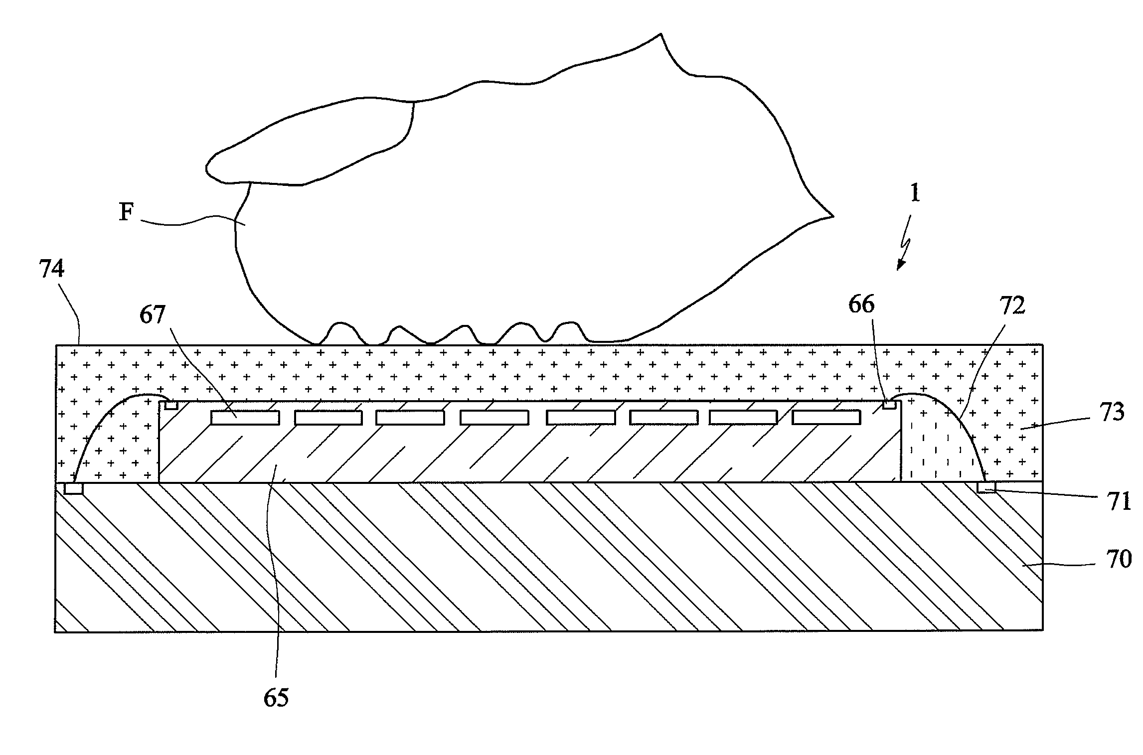
[0031]FIG. 3 is a schematic illustration showing a structure of a capacitive sensing array device 1 according to a first embodiment of the invention. FIG. 4 is a schematic illustration partially showing a structure design of sensing electrodes of the capacitive sensing array device 1 according to the first embodiment of the invention. FIG. 5 is a schematic illustration showing a single sensing member and its corresponding sensing circuit of the capacitive sensing array device 1 according to the first embodiment of the invention. Referring to FIGS. 3 to 5, the capacitive sensing array device 1 of this embodiment includes sensing electrodes 10, a shielding conductor layer 20, a coupling signal source 30, a constant voltage source 40, switch modules 50, a semiconductor substrate 65, a pa...


PUM


Abstract

A capacitive sensing array device of an electronic apparatus includes sensing electrodes, a shielding conductor layer, a coupling signal source, a constant voltage source and switch modules. The coupling signal source provides a coupling signal coupled to an object. The constant voltage source provides a constant voltage to the shielding conductor layer to form a stable vertical parasitic capacitor between the shielding conductor layer and each sensing electrode. Each switch module is electrically connected to the constant voltage source via the corresponding sensing electrode. When one sensing electrode is selected to perform sensing, the corresponding switch module is configured as an open-circuited state such that the selected sensing electrode is disconnected from the constant voltage source, while the other sensing electrodes are electrically connected to the constant voltage source to form a stable horizontal parasitic capacitor between the selected sensing electrode and the other sensing electrodes.

Description

[0001]This application claims priority of No. 101137686 filed in Taiwan R.O.C. on Oct. 12, 2012 under 35 USC 119, the entire content of which is hereby incorporated by reference.BACKGROUND OF THE INVENTION[0002]1. Field of the Invention[0003]The invention relates to a capacitive sensing array device and an electronic apparatus using the same, and more particularly to a capacitive sensing array device with high sensitivity and an electronic apparatus using the same.[0004]2. Related Art[0005]The conventional capacitive sensing technology for sensing the skin of the human body may be applied to, for example, the fingerprint sensor for sensing finger's textures or a capacitive touch panel or a capacitive touch screen.[0006]More particularly, the basic structure of the portion of the sensor in contact with the skin's texture to sense the skin's texture is an array-type sensing member. That is, several sensing members with the same structures constitute a two-dimensional array sensor. Whe...

Claims


Application Information

Patent Timeline
Patent Type & Authority Patents(United States)
IPC IPC(8): G01R27/26G06F3/041G06F3/044G01R1/00G06F1/00H03K17/96
CPCG01R27/2605G06F3/044G06F3/0416G01R1/00G06F1/00G06F2101/00H03K17/9622H03K2217/960705G06F3/04166G06F3/0443H01L2224/48091H01L2924/00014
Inventor CHOU, BRUCE C.S.HSU, SHIH CHIEH
Owner J METRICS TECH CO LTD
Why Eureka
Try Eureka