Apparatuses and methods for asymmetric input/output interface for a memory

Active Publication Date: 2018-05-08
MICRON TECH INC
View PDF15 Cites 1 Cited by
  • Summary
  • Abstract
  • Description
  • Claims
  • Application Information

AI Technical Summary

Benefits of technology

The patent describes a memory controller that can be made using a fast logic fabrication process. This process produces transistors that are faster and more sensitive, allowing the memory controller to operate at higher speeds. The transmitters can drive data signals with larger voltage swings, and the receivers can detect signals with lower voltage swings. This means that the memory controller can handle large amounts of data at high speeds.

Problems solved by technology

This system clock may determine input / output (I / O) speeds of the host system and may also be limited by the slowest device in the system.
For other devices, however, a system clock that begins to reach their maximum internal operating speeds begins to pose problems for I / O operations.
Other devices, on the other hand, may have comparatively slower transistors, which may result in comparatively slower internal operating rates and I / O rates.
Further, the output circuits may drive large voltage swing signals at comparatively slow slew rates.
As a consequence, a maximum I / O rate the output circuits are capable of reaching may be limited due to the slew rate.
At higher I / O rates, a memory output circuit may not be able to reach the designed output voltage swing due to the limited slew rate during a clock cycle.
As such, a device receiving outputs from the memory, e.g., a memory controller or a system on a chip, may not receive reliable signals at those higher I / O rates.

Method used


Image

  • Apparatuses and methods for asymmetric input/output interface for a memory
  • Apparatuses and methods for asymmetric input/output interface for a memory
  • Apparatuses and methods for asymmetric input/output interface for a memory

Examples


Embodiment Construction

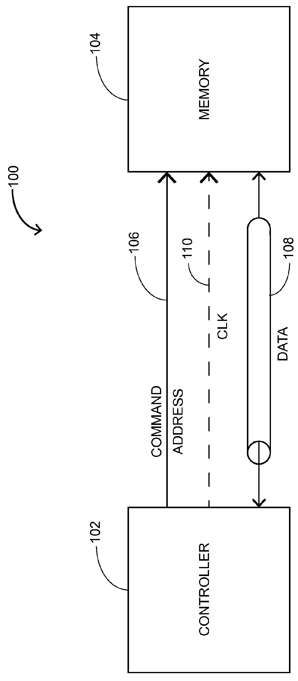
[0009]Apparatuses and methods for an asymmetric input / output interface for a memory are disclosed herein. Certain details are set forth below to provide a sufficient understanding of embodiments of the disclosure. However, it will be clear to one having skill in the art that embodiments of the disclosure may be practiced without these particular details. Moreover, the particular embodiments of the present disclosure described herein are provided by way of example and should not be used to limit the scope of the disclosure to these particular embodiments. In other instances, well-known circuits, control signals, timing protocols, and software operations have not been shown in detail in order to avoid unnecessarily obscuring the disclosure.

[0010]As discussed above, various devices (e.g., integrated circuits such as logic devices, memory controllers, systems on a chip, processors, and memories) of an electronic system may perform at varying rates, such as internal operation rates and I...


PUM


Abstract

Apparatuses and methods for asymmetric input / output interfaces for memory are disclosed. An example apparatus may include a receiver and a transmitter. The receiver may be configured to receive first data signals having a first voltage swing and having a first slew rate. The transmitter may be configured to provide second data signals having a second voltage swing and having a second slew rate, wherein the first and second voltage swings are different, and wherein the first and second slew rates are different.

Description

BACKGROUND[0001]Most electronics systems include multiple devices communicating with one another via a connection, such as conductive traces on a printed circuit board on which the devices are mounted or conductive traces connecting different areas of an integrated circuit on a single die. While the various devices included in an electronics system may be internally operating at different speeds, the communications that occur between the devices may be operating based on a system clock. This system clock may determine input / output (I / O) speeds of the host system and may also be limited by the slowest device in the system. For some devices, a logic device for example, a fast system clock may pose no problems because the internal components of the device, e.g., transistors, may operate based on a higher clock rate than the system clock. For other devices, however, a system clock that begins to reach their maximum internal operating speeds begins to pose problems for I / O operations.[00...

Claims


Application Information

Patent Timeline
IPC IPC(8): G06F13/16G06F13/40
CPCG06F13/4068G06F13/1689G06F13/1694
InventorGANS, DEANSCHOBER, BRUCECHAE, MOO SUNG
OwnerMICRON TECH INC