
Quantum dot photoelectric detector and preparation method thereof
A technology of photodetectors and quantum dots, applied in the field of photodetectors, can solve the problems of poor sensitivity of photodetectors, short mean free path of electron scattering, and limited absorption spectrum range of quantum dot photodetectors, etc., achieving convenient and flexible application, The preparation method is simple and the effect of high sensitivity
Patent Information
- Authority / Receiving Office
- CN · China
- Patent Type
- Applications(China)
- Current Assignee / Owner
- Publication Date
- 2021-06-29
Smart Images
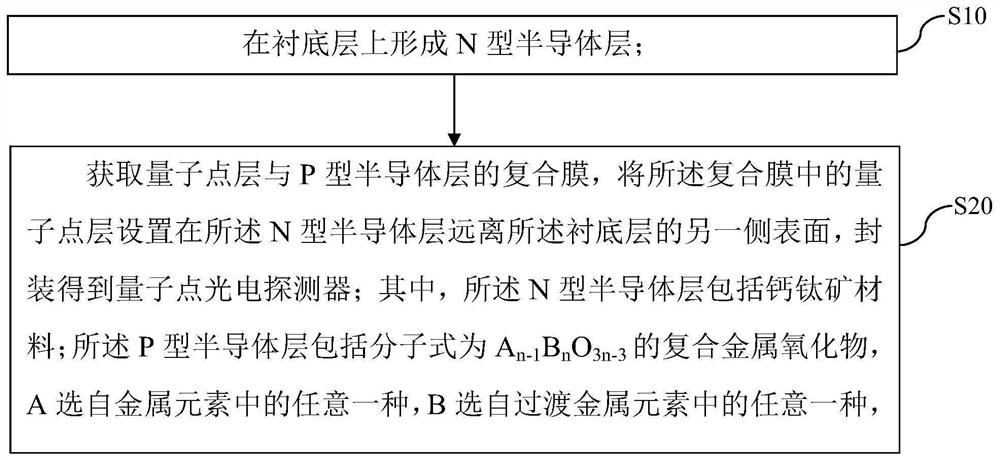
Figure 1 
Figure 2
Abstract
Description
technical field
[0001] The invention belongs to the technical field of photodetectors, in particular to a quantum dot photodetector and a preparation method thereof. Background technique
[0002] Converting optical signals to electrical signals is still a cutting-edge technology that needs to be solved urgently, and it has a wide range of applications in real life, such as video imaging, optical communication, biomedical imaging, night photography, motion detection, etc. Photodetectors are the most basic electronic devices in these common applications. The function of photodetectors is to convert optical signals into electrical signals, which is equivalent to a converter of energy signals, and the final output is electrical signals. In addition to converting optical signals into electrical signals, general optoelectronic systems can also perform targeted processing on electrical signals according to different needs, and store them and apply them in various fields, such as: i...
Examples
preparation example Construction
[0033] Correspondingly, as attached figure 1 As shown, the embodiment of the present invention also provides a method for preparing a quantum dot photodetector, comprising the following steps:
[0034] S10. forming an N-type semiconductor layer on the substrate layer;
[0035] S20. Obtain a composite film of a quantum dot layer and a P-type semiconductor layer, arrange the quantum dot layer in the composite film on the surface of the other side of the N-type semiconductor layer away from the substrate layer, and package to obtain quantum dot photodetection device;
[0036] Wherein, the N-type semiconductor layer includes a perovskite material; the P-type semiconductor layer includes a compound with the molecular formula A n- 1 B n o 3n-3 A composite metal oxide, A is selected from any one of the metal elements, B is selected from any one of the transition metal elements, n≥3.
[0037] The preparation method of the quantum dot photodetector provided by the embodiment of t...
Embodiment 1
[0067] A quantum dot photodetector comprising the following preparation steps:
[0068] 1. Doping 0.001g niobium nitrate into 1g SrTiO 3 In aqueous solution, SrTiO doped with niobium was prepared 3 The base layer was then transferred onto indium tin oxide glass.
[0069] 2. Spin-coat the 5mg / ml CdSe / ZnS quantum dot solution on the copper flake layer, and anneal at a low temperature of 40 degrees Celsius to form a thin film.
[0070]3. Spin-coat the ethyl lactate solution on the quantum dot layer at 100 r / min, and heat to 60 degrees Celsius for 5 hours.
[0071] 4. After the above step 3 is completed, spin coat a layer of polymethyl methacrylate on the ethyl lactate layer at 500r / min.
[0072] 5. Will be Bi 2 Fe 3 o 6 After the aqueous solution was passed through nitrogen for 1 hour, it was heated to 50 degrees Celsius and then spin-coated on the polymethyl methacrylate layer at a speed of 1000 r / min.
[0073] 6. After the above steps are completed, etch off the copper f...
Embodiment 2
[0077] A quantum dot photodetector comprising the following preparation steps:
[0078] 1. Doping 0.0001g of yttrium nitrate into 1g of BaTiO 3 In aqueous solution, BaTiO doped with yttrium was prepared 3 The base layer was then transferred onto indium tin oxide glass.
[0079] 2. Spin-coat 10mg / ml CdSeSTe quantum dot solution onto the copper flake layer, and anneal at a low temperature of 40 degrees Celsius to form a thin film.
[0080] 3. Spin-coat the ethyl lactate solution on the quantum dot layer at 400r / min, and heat to 80°C for 1 hour.
[0081] 4. After the above step 3 is completed, spin coat a layer of polymethyl methacrylate on the ethyl lactate layer at 1000r / min.
[0082] 5. Will be Pb 3 Fe 4 o 8 After the aqueous solution was passed through nitrogen for 1 hour, it was heated to 50 degrees Celsius and then spin-coated on the polymethyl methacrylate layer at a speed of 8000 r / min.
[0083] 6. After the above steps are completed, etch off the copper thin film ...