
Semiconductor device and manufacturing method of the same
Patent Information
- Authority / Receiving Office
- US · United States
- Current Assignee / Owner
- Publication Date
- 2006-09-07
- Estimated Expiration
- Not applicable · inactive patent
Smart Images
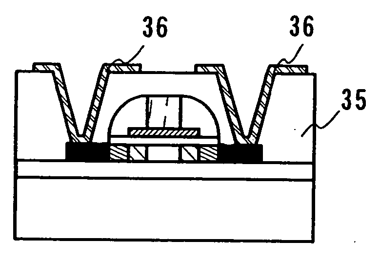
Figure 1 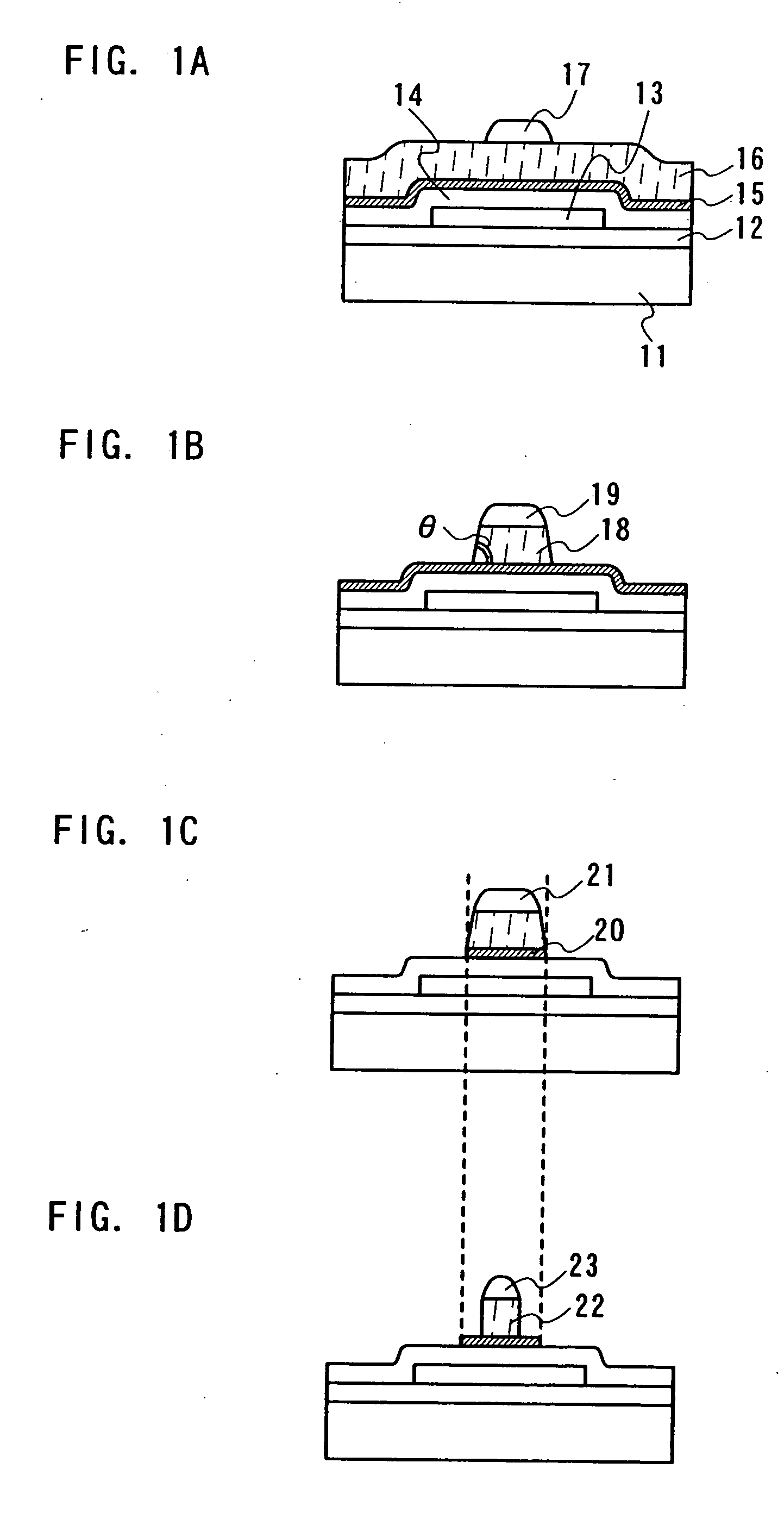
Figure 2 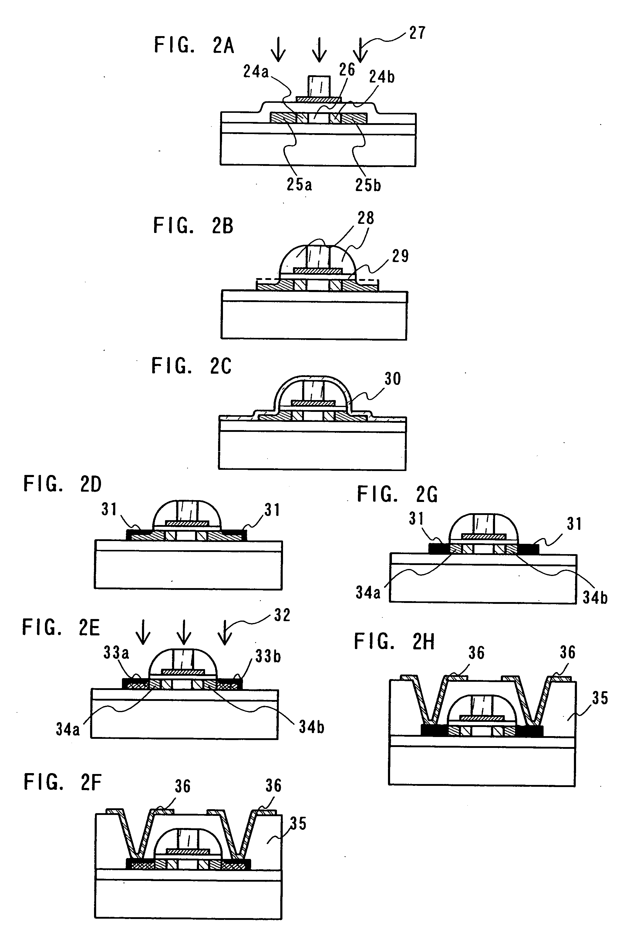
Figure 3
Abstract
Description
BACKGROUND OF THE INVENTION
[0001] 1. Field of the Invention
[0002] The present invention relates to a semiconductor device forming various circuits and a manufacturing method of the semiconductor device.
[0003] 2. Related Art
[0004] A conventional thin film transistor (hereinafter, referred to as a TFT) is formed by using an amorphous semiconductor film; therefore, it was almost impossible to obtain a TFT having field effect mobility of 10 cm2 / V·Sec or more. However, a TFT having high filed effect mobility can be obtained owing to the appearance of a TFT formed by using a crystalline semiconductor film.
[0005] Since the TFT formed by using a crystalline semiconductor film has high field effect mobility, various functional circuits can be formed over the same substrate concurrently by using the TFT. For example, in a display device, a driver IC and the like are mounted on a display portion to have a driver circuit previously. On the other hand, by using the TFTs formed by using crys...
Examples
embodiment 1
[0074] Hereinafter, a method for manufacturing a semiconductor device in accordance with Embodiment 1 will be described with reference to FIGS. 1A to 1D, 2A to 2H, 3A to 3D, and 4A to 4C. A TFT used in the semiconductor device of the present embodiment has a Lov region and a Loff region as an LDD region.
[0075] First, over a substrate 11, a base insulating film 12 is formed to be 100 to 300 nm thick. As the substrate 11, an insulating substrate such as a glass substrate, a quartz substrate, a plastic substrate or a ceramic substrate; a metal substrate; a semiconductor substrate; or the like can be used.
[0076] The base insulating film 12 can be formed by using a single layer structure of an insulating film containing oxygen or nitrogen such as silicon oxide (SiOx), silicon nitride (SiNx), silicon oxide containing nitrogen (SiOxNy) (x>y) (also referred to as silicon oxynitride), or silicon nitride containing oxygen (SiNxOy) (x>y) (also referred to as silicon nitride oxide), or a stak...
embodiment 2
[0121] In the present embodiment, a method for manufacturing a semiconductor device having only a Lov region will be described with reference to FIG. 5A to 5F. Further, in the present embodiment, the same reference numerals are used for the same portions as in Embodiment 1, and a detailed explanation is omitted.
[0122] In the present embodiment, a TFT is manufactured through the same steps as in Embodiment 1 until the step of FIG. 2A. Subsequently, doping of an impurity ion 32 is conducted by using a first electrode 20 as a mask to form high concentration impurity regions 52a and 52b (FIG. 5A). In addition, doping of the impurity ion 32 for forming the high concentration impurity region and doping of an impurity ion 27 for forming the low concentration impurity region may be conducted in the reverse order; namely, doping of the impurity ion 27 may be conducted after doping of the impurity ion 32, and a state of FIG. 5A is obtained. Alternatively, doping of the impurity ion 27 may be...
embodiment 3
[0131] In the present embodiment, a method for manufacturing a semiconductor device having only a Loff region will be described with reference to FIGS. 6A to 6F. Further, in the present embodiment, the same reference numerals are used for the same portions as in Embodiments 1 and 2, and a detailed explanation is omitted.
[0132] The same steps as in Embodiment 2 are conducted until FIG. 5A, and low-concentration impurity regions 24a and 24b, high-concentration impurity regions 52a and 52b, and a channel formation region 26 are formed in an island-shaped semiconductor film 13. Then, by using a second gate electrode 22 as a mask, dry etching is conducted to etch a first gate electrode and a gate insulating film 14 so as to have the same width as the gate length of the second gate electrode. By this etching, a third gate electrode 62 and a gate insulating film 61 are formed, and a part of the island-shaped semiconductor film 13 is exposed (FIG. 6A).
[0133] Subsequently, an insulating fi...