Bidirectional shift register

A shift register, reset signal technology, applied in static memory, digital memory information, instruments, etc., can solve problems such as time required

Inactive Publication Date: 2009-09-02
SEIKO EPSON CORP
View PDF4 Cites 0 Cited by
  • Summary
  • Abstract
  • Description
  • Claims
  • Application Information

AI Technical Summary

Problems solved by technology

Therefore, for example, when using the above-mentioned bidirectional shift register as a data line driving circuit, when the design is changed, it is necessary to consider the change in the pulse width of the output signal, and the design work takes time.

Method used


Image

  • Bidirectional shift register
  • Bidirectional shift register
  • Bidirectional shift register

Examples


Embodiment Construction

[0113]

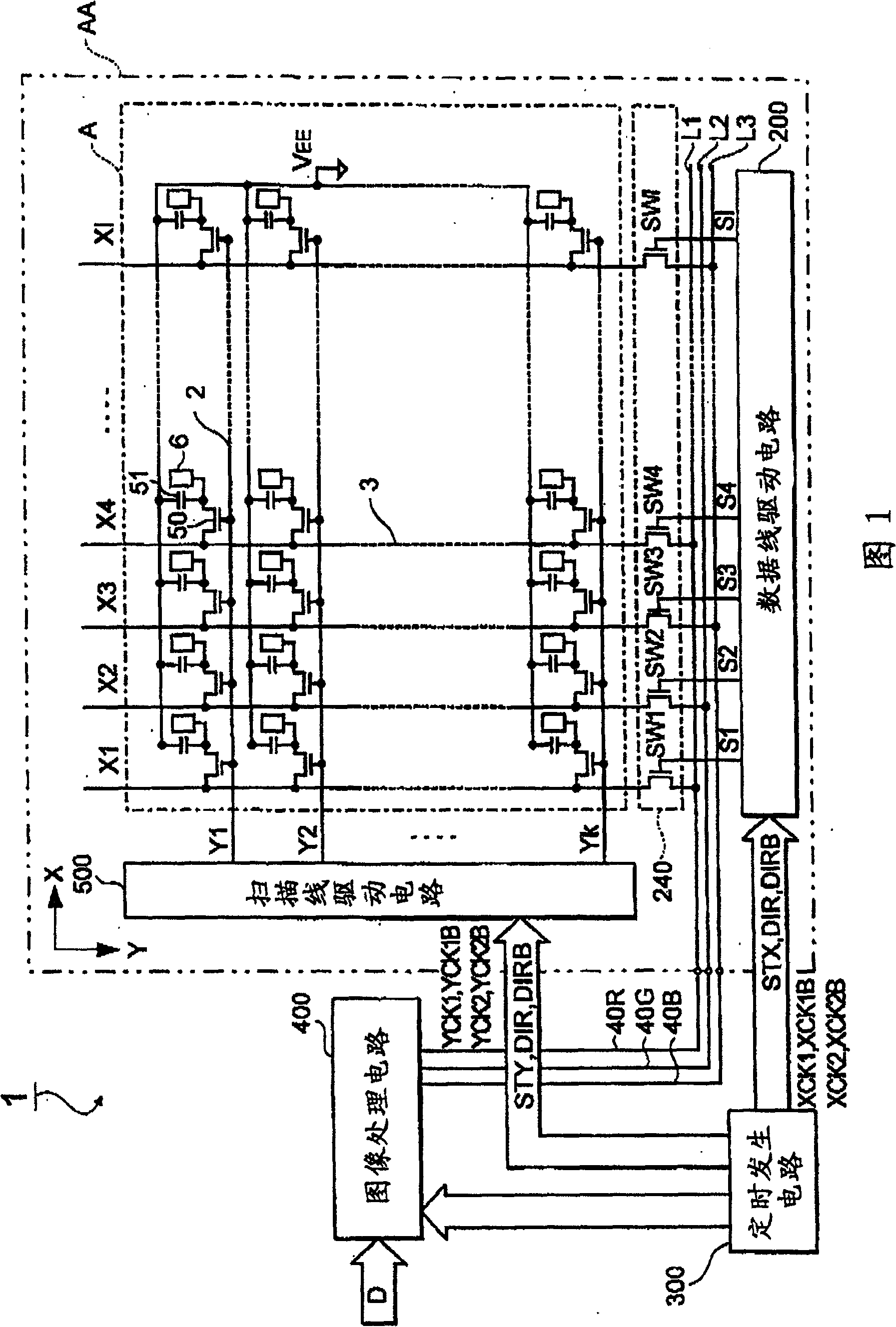
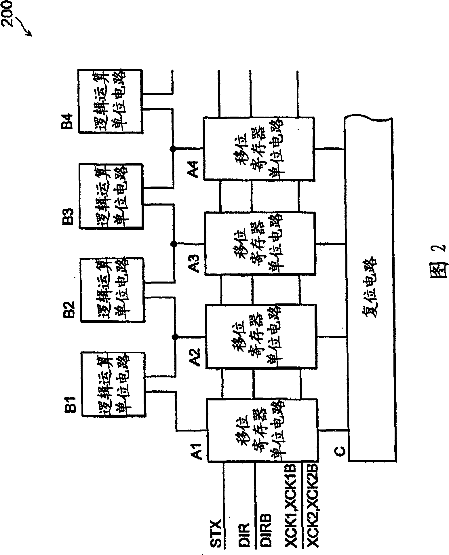
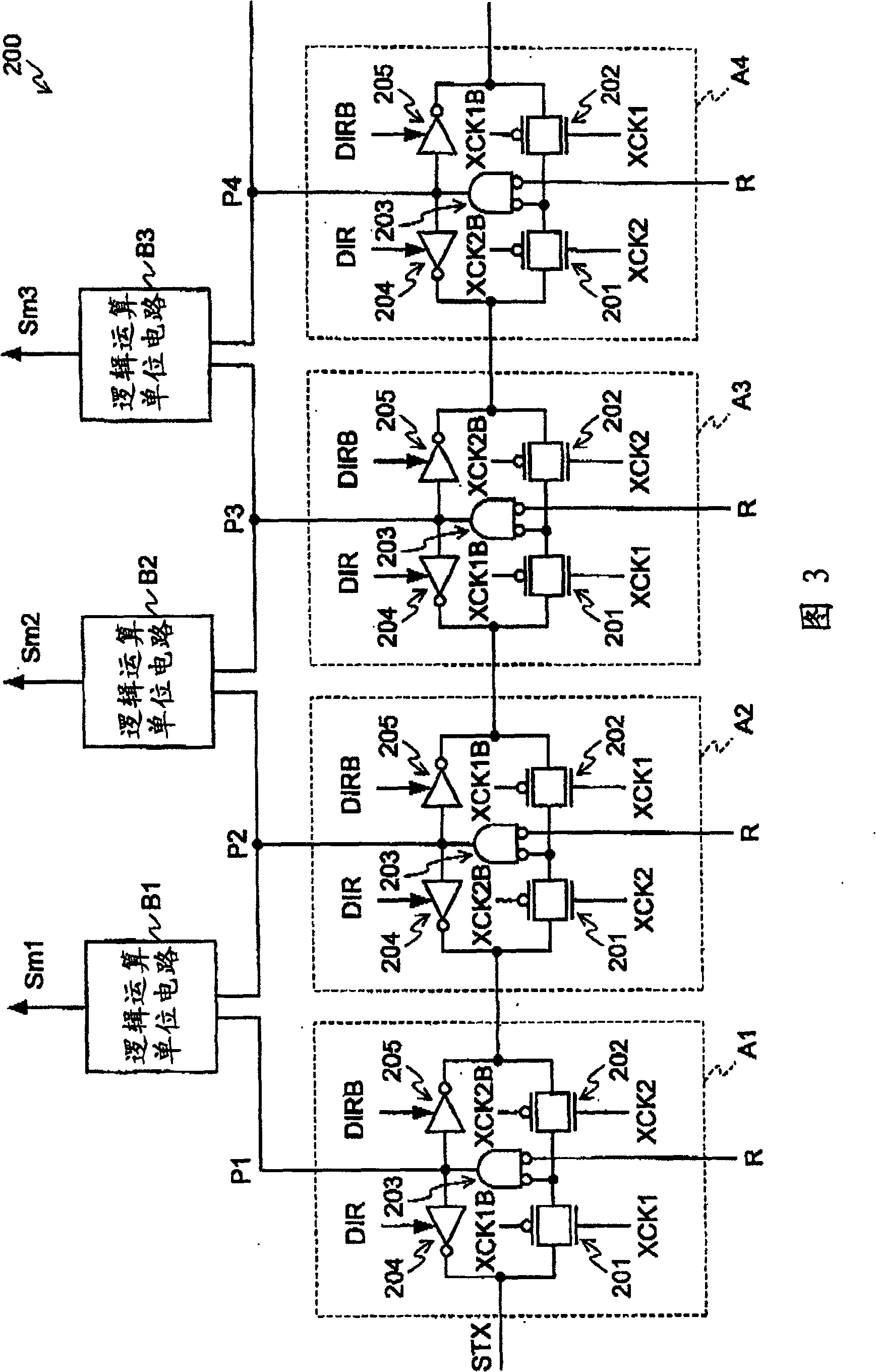
[0114] figure 1 It is a block diagram showing the overall configuration of the electro-optical device 1 to which the data line drive circuit 200 serving as the bidirectional shift register of the present embodiment is applied.

[0115] First, the electro-optical device 1 uses liquid crystal as an electro-optic material. This electro-optical device 1 has a liquid crystal panel AA as a main part. The liquid crystal panel AA has, as a switching element, an element substrate on which a thin film transistor (hereinafter referred to as "TFT") is formed as a switching element, an opposing substrate arranged to face the element substrate at a certain interval, and an element substrate between these element substrates. and the liquid crystal disposed between the opposing substrates.

[0116] The electro-optical device 1 includes a timing generation circuit 300 and an image processing circuit 400 in addition to the liquid crystal panel AA. The element substrate of the liq...


PUM


Abstract

The present invention provides a bidirectional shift register which makes output signal pulse widths the same regardless of whether it is constituted by positive logic or negative logic. A data line driving circuit (200) has a multi-stage shift register unit circuit (A). The shift register unit circuit (A) has first and second transmission gates (201, 202) for synchronously transmitting the X transmission start pulse STX with the X clock signal XCK and the inverted X clock signal XCKB, and a second transmission gate (201, 202) for inverting the input signal and outputting it. A logic circuit (203) and a logic level of the corresponding transfer direction control signal DIR are mutually exclusive of the first and second clock-controlled inverters (204, 205) that become valid. The output end of the first logic circuit (203) is connected to the input end of the clock control type inverter (204, 205), and the output end of the clock control type inverter (204, 205) is connected to the transmission gate (201, 202) and The input terminal of the first logic circuit (203) is connected.

Description

technical field [0001] The present invention relates to a bidirectional shift register, which can be applied to, for example, data line driving circuits and scanning line driving circuits of liquid crystals, electro-optical devices and electronic equipment using these driving circuits. Background technique [0002] Conventionally, a liquid crystal display device is known as an electro-optical device that displays an image in an image display area. This liquid crystal display device includes, for example, a data line driver circuit and a scan line driver circuit for supplying data line signals, scan signals, and the like to data lines and scan lines wired in an image display region at predetermined timings. Such a data line driving circuit and a scanning line driving circuit have a bidirectional shift register that outputs a sampling signal, and write an image signal into each pixel based on the sampling signal. [0003] <1: The structure of the bidirectional shift regist...

Claims


Application Information

Patent Timeline
Patent Type & Authority Patents(China)
IPC IPC(8): G11C19/28G09G3/36
CPCG11C19/28G09G3/3688G09G3/3677G09G2310/0283G09G3/20G11C19/00H03K19/00
Inventor 片山茂宪
Owner SEIKO EPSON CORP
Why Eureka
Try Eureka