Optical sensing device and display with optical sensing device

A technology of light sensing and illuminance, applied in static indicators, instruments, data processing input/output process, etc., can solve the problems of increasing cost, complex circuit structure, reducing display aperture ratio, etc.

Inactive Publication Date: 2010-07-07
AU OPTRONICS CORP
View PDF0 Cites 23 Cited by
  • Summary
  • Abstract
  • Description
  • Claims
  • Application Information

AI Technical Summary

Problems solved by technology

Because the prior art needs to add an additional control signal to the existing circuit of the pixel unit, the circuit structure is relatively complicated.
However, an overly complex circuit architecture will increase the difficulty of wiring thin film transistors and increase the cost
[0005] Furthermore, since the light sensing signal is usually quite weak,

Method used


Image

  • Optical sensing device and display with optical sensing device
  • Optical sensing device and display with optical sensing device
  • Optical sensing device and display with optical sensing device

Examples


no. 1 example

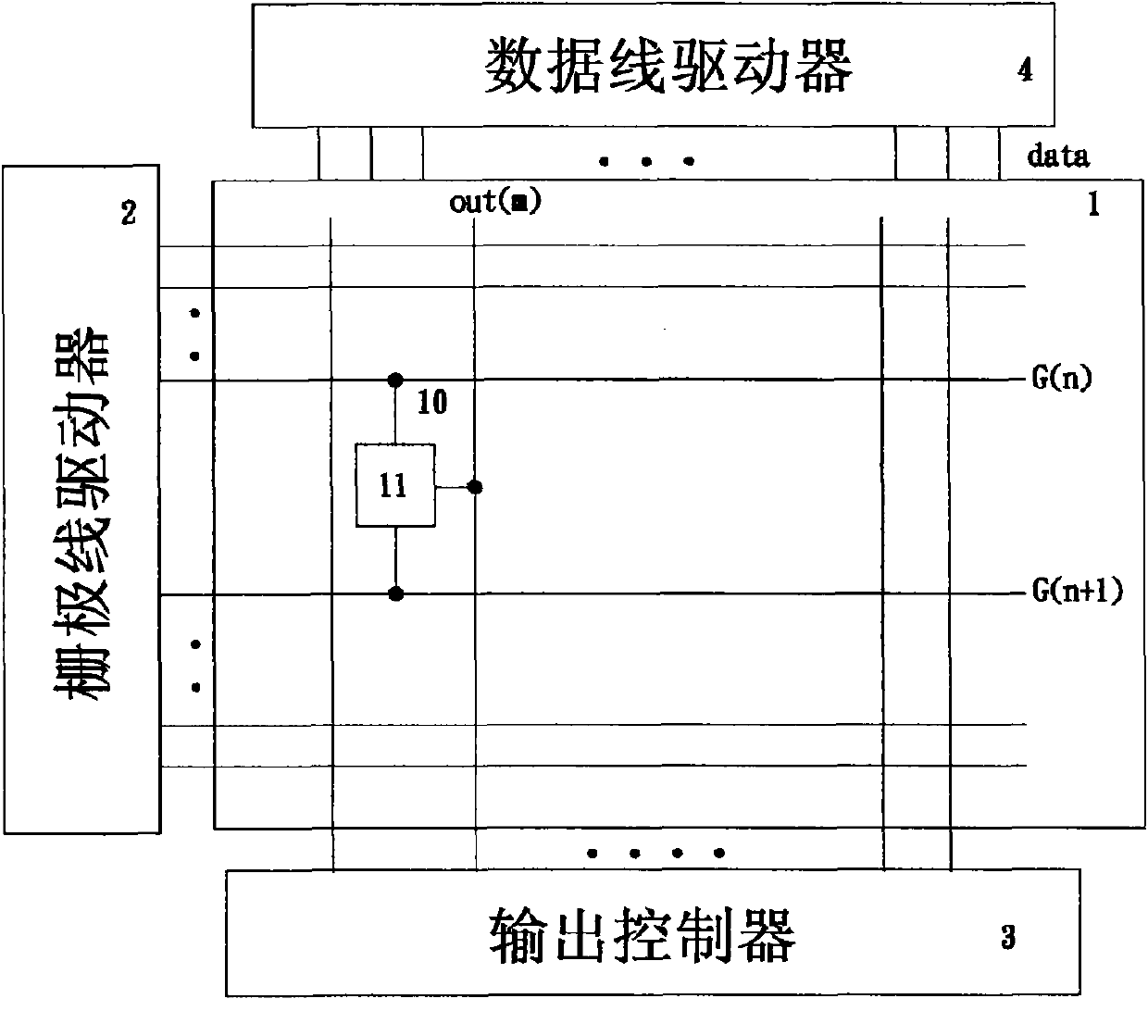
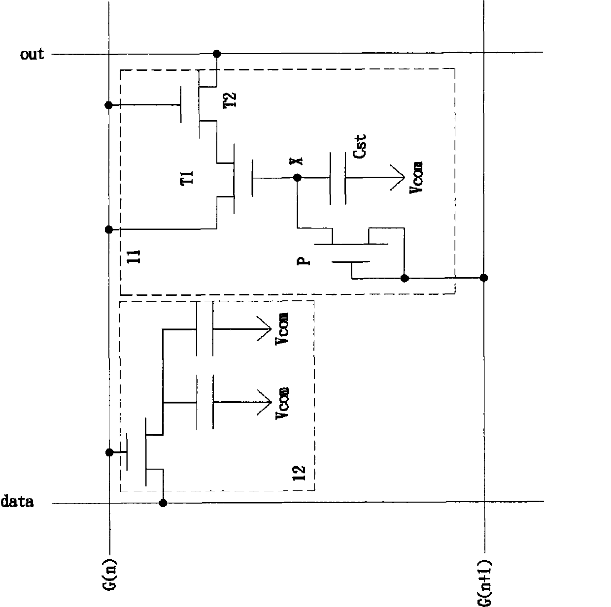
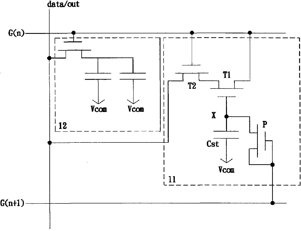
[0024] see Figure 2A , which shows a schematic diagram of the first embodiment of the light sensing device of the present invention. Each of the light-sensing devices 11 of the present invention is electrically connected to an adjacent first gate line G(n), a second gate line G(n+1) and an output line out; the light-sensing The detection device 11 includes: a light sensing element P, a storage capacitor Cst, a first thin film transistor T1 and a second thin film transistor T2. Wherein, one end of the photo-sensing component P is electrically connected to the second gate line G(n+1), and the other end defines a node X; the photo-sensing component P can be any Components of electrical signals, such as photodiodes or photo thin film transistors. Such as Figure 2A In the first embodiment shown, the light sensing element P can be a photoelectric thin film transistor, one of its gate and source / drain is electrically connected to the second scanning line G(n+1), and the other is...


PUM


Abstract

The invention provides an optical sensing device, which comprises an optical sensing component, a storage capacitor, a first thin-film transistor and a second thin-film transistor. The optical sensing component can reset the voltage of a node as a first voltage level, and the storage capacitor is electrically connected with the node to discharge the node to a second voltage level within frame time according to the intensity of illumination of the optical sensing component. The second voltage level controls the conduction voltage of the first thin-film transistor, and the second thin-film transistor outputs a voltage to be read according to the conduction voltage.

Description

【Technical field】 [0001] The present invention relates to a light sensing device, in particular to a light sensing device capable of increasing the aperture ratio of a display; the present invention also relates to a display with the above light sensing device. 【Background technique】 [0002] With the vigorous development of technology, network, and communication, electronic products not only need to have the novelty of technology, but also seek direct interaction with users to meet the needs of users in terms of convenience and interactivity. Therefore, many touch-sensitive products and interfaces have been launched correspondingly, such as ATM cash machines, personal digital assistants (Personal Digital Assistant, PDA), mobile phones or notebook computers. The touch-sensitive products allow the user to approach or press the touch panel (touch panel) to directly interact between the user and the electronic product to complete data transmission, access and update, thus incre...

Claims


Application Information

Patent Timeline
IPC IPC(8): G06F3/042G02F1/133
Inventor 陈勇志苏国彰徐国华刘俊欣
Owner AU OPTRONICS CORP
Why Eureka
Try Eureka