Method for separating a semiconductor wafer into individual semiconductor dies using an implanted impurity

A technology of semiconductor tubes and semiconductors, used in semiconductor/solid-state device manufacturing, electrical components, circuits, etc.

Inactive Publication Date: 2010-08-18
AGERE SYST INC
View PDF6 Cites 0 Cited by
  • Summary
  • Abstract
  • Description
  • Claims
  • Application Information

AI Technical Summary

Problems solved by technology

However, there are practical limitations to reducing the blade or scribing tool thickness to obtain a narrower kerf

Method used


Image

  • Method for separating a semiconductor wafer into individual semiconductor dies using an implanted impurity
  • Method for separating a semiconductor wafer into individual semiconductor dies using an implanted impurity
  • Method for separating a semiconductor wafer into individual semiconductor dies using an implanted impurity

Examples


Embodiment Construction

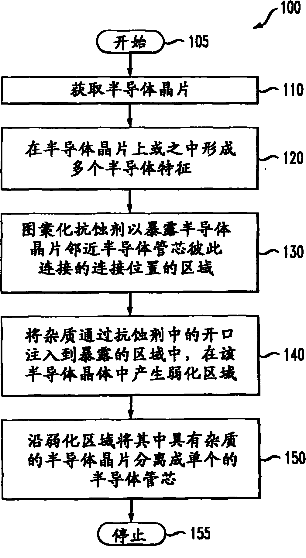
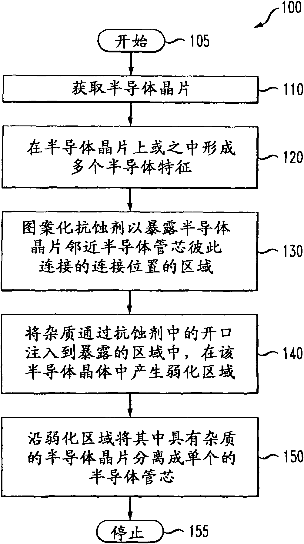
[0010] The present disclosure is based at least in part on the recognition that impurities may be implanted into a semiconductor wafer adjacent to connection locations where semiconductor die are interconnected to facilitate separation of the semiconductor wafer into individual semiconductor dies. The present disclosure also recognizes that implanted impurities can break bonds in the semiconductor wafer adjacent to the connection locations, creating regions of weakness along which the semiconductor wafer can be separated into individual semiconductor dies.

[0011] FIG. 1 shows a flowchart 100 representing an embodiment of a method for fabricating a semiconductor die. In addition to methods for fabricating semiconductor dies, the flowchart includes a subset of methods for separating a semiconductor wafer into individual semiconductor dies. Accordingly, flowchart 100 should not be used to limit the disclosure to any particular steps.

[0012] Flowchart 100 begins with start st...


PUM

PropertyMeasurementUnit
Widthaaaaaaaaaa

Abstract

Provided is a method for separating a semiconductor wafer into individual semiconductor dies. The method for separating the semiconductor wafer, among other steps, may include implanting an impurity into regions of a semiconductor wafer proximate junctions where semiconductor dies join one another, the impurity configured to disrupt bonds in the semiconductor wafer proximate the junctions and lead to weakened regions. The method for separating the semiconductor wafer may further include separating the semiconductor wafer having the impurity into individual semiconductor dies along the weakened regions.

Description

technical field [0001] The present invention generally relates to a method of separating a semiconductor wafer into individual semiconductor dies, and more particularly, to a method of separating a semiconductor wafer into individual semiconductor dies using implanted impurities, and a method of manufacturing semiconductor wafers using implanted impurities. Die method. Background technique [0002] During the fabrication of integrated circuits, multiple integrated circuits (semiconductor dies) are formed simultaneously on a single semiconductor wafer through a series of material deposition and removal processes. The individual semiconductor dies are then separated from the wafer in a process known as dicing. Wafer dicing typically involves sawing the wafer with a circular saw blade or by scribing and breaking the wafer (if the wafer is crystalline). The portion of the semiconductor wafer where the dies are separated is known as an incision, or in semiconductor manufacturin...

Claims


Application Information

Patent Timeline
IPC IPC(8): H01L21/78H01L21/265
CPCH01L21/78
Inventor E·B·哈里斯K·G·斯坦纳
Owner AGERE SYST INC
Why Eureka
Try Eureka