Liquid crystal display and manufacturing method thereof

A technology of liquid crystal display and manufacturing method, which is applied in semiconductor/solid-state device manufacturing, static indicators, instruments, etc., can solve the problems of limited single-sided display and inconspicuous effect, reduce power consumption, increase display content, reduce Effects of Environmental Pollution

Active Publication Date: 2011-04-20
BOE TECH GRP CO LTD +1
View PDF0 Cites 21 Cited by
  • Summary
  • Abstract
  • Description
  • Claims
  • Application Information

AI Technical Summary

Problems solved by technology

Since the power consumption of the backlight accounts for more than 2 / 3 of the overall power consumption of the liquid crystal display, some technical solutions have been proposed in the prior art to use photosensitive devices to adjust the brightness of the backlight according to the intensity of ambient light to reduce power consumption, but the effect is not obvious.
In addition, the prior art has also proposed some technical methods for semi-transmissive and semi-reflective liquid crystal displays, but they are all limited to single-sided display.

Method used


Image

  • Liquid crystal display and manufacturing method thereof
  • Liquid crystal display and manufacturing method thereof
  • Liquid crystal display and manufacturing method thereof

Examples


Embodiment Construction

[0052] The technical solutions of the present invention will be further described in detail below through the accompanying drawings and embodiments. The thickness of each layer and the size and shape of the area in the drawings do not reflect the true proportions of the liquid crystal display, TFT-LCD array substrate or color film substrate, and are only intended to illustrate the content of the present invention.

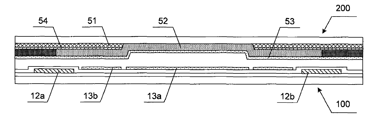
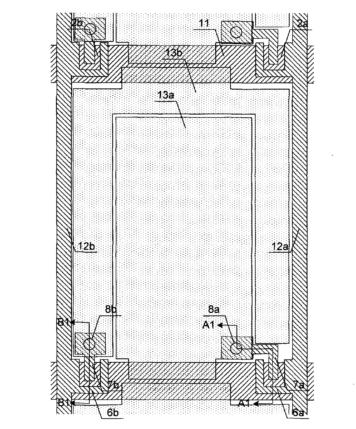
[0053] figure 1 It is a schematic diagram of the structure of the liquid crystal display of the present invention. Such as figure 1 As shown, the main structure of the liquid crystal display of the present invention includes a TFT-LCD array substrate 100 and a color filter substrate 200 that are aligned together and sandwich liquid crystals therebetween. Gate lines, first data lines 12a and second data lines 12b are formed on the TFT-LCD array substrate 100 of the present invention. The adjacent gate lines and the first data lines 12a and the second data lines 12b def...


PUM

PropertyMeasurementUnit
thicknessaaaaaaaaaa
thicknessaaaaaaaaaa

Abstract

The invention relates to a liquid crystal display and a manufacturing method thereof. The liquid crystal display comprises a TFT-LCD array substrate and a color film substrate which are covered together, wherein the TFT-LCD array substrate comprises a grid line, a first thin film transistor for controlling a first data line to supply a first pixel electrode with a first data voltage, and a secondthin film transistor for controlling a second data line to supply a second pixel electrode with a second data voltage; the color film substrate comprises black matrixes and color resins; the positionof the first pixel electrode is corresponded to the position of the color resin between the black matrixes; a first image is displayed at one side of the color film substrate in the manner of transmission; the position of the second pixel electrode is corresponded to the position of the color resin on the black matrix; and a second image is displayed on one side of the TFT-LCD array substrate in the manner of transmission. A double pixel structure is arranged in the liquid crystal display provided by the invention and the semi-transmission and semi-reflection designs are adopted, so the content of two frames can be respectively displayed and the display content of the display device is increased.

Description

Technical field [0001] The invention relates to a display and a method for manufacturing the display, in particular to a liquid crystal display and a manufacturing method thereof. Background technique [0002] The main structure of the Thin Film Transistor Liquid Crystal Display (TFT-LCD) includes a cell array substrate and a color film substrate. The array substrate has gate lines, data lines, and thin film transistors arranged in a matrix. Pixel electrode, black matrix, color resin and common electrode are formed on the color filter substrate. The liquid crystal molecules are deflected by controlling the voltage difference between the pixel electrode of the array substrate and the common electrode of the color filter substrate. The light source emitted from the backlight passes through the liquid crystal It modulates light with different gray levels to display different images. [0003] Currently, existing liquid crystal displays generally need to use a backlight source for disp...

Claims


Application Information

Patent Timeline
Patent Type & Authority Applications(China)
IPC IPC(8): G02F1/1362G02F1/1368H01L27/02H01L21/82H01L21/50
CPCG02F1/133555G02F1/133512G02F1/13624G02F2001/136236H01L29/41733G02F1/136213G09G3/3688H01L27/1214G09G3/3648G02F2001/133342G02F1/133342G02F1/136236H01L27/124
Inventor 王峥
Owner BOE TECH GRP CO LTD
Why Eureka
Try Eureka