Supercharge Your Innovation With Domain-Expert AI Agents!

Thermosetting adhesive film, adhesive film with dicing film, and manufacturing method of semiconductor apparatus using the thermosetting adhesive film or the adhesive film with dicing film

A technology for gluing films and cutting films, which is used in film/sheet adhesives, semiconductor devices, semiconductor/solid-state device manufacturing, etc. Reliability decline and other problems, to achieve the effect of improving manufacturing efficiency

Active Publication Date: 2011-08-17
NITTO DENKO CORP
View PDF5 Cites 14 Cited by
  • Summary
  • Abstract
  • Description
  • Claims
  • Application Information

AI Technical Summary

Problems solved by technology

However, if no filler is added, the tensile storage elastic modulus of the die-bonding film may decrease, resulting in a new problem of lowering the reliability of the package.
In addition, if no filler is added, the thermal shrinkage of the die-bonding film during thermal curing may cause warping and damage of the semiconductor chip
[0008] In addition to not being limited to die-bonding films, when thermosetting adhesive films are configured without adding fillers, the tensile storage elastic modulus may decrease, or thermal shrinkage may occur during thermosetting.

Method used

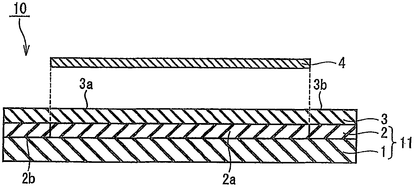
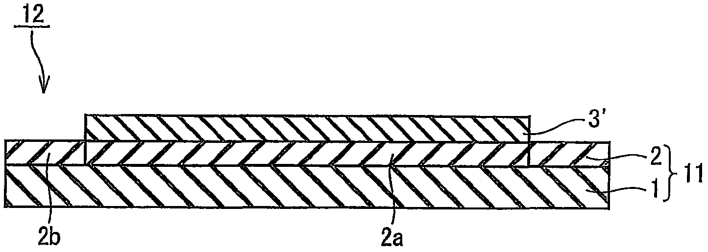

Image

  • Thermosetting adhesive film, adhesive film with dicing film, and manufacturing method of semiconductor apparatus using the thermosetting adhesive film or the adhesive film with dicing film
  • Thermosetting adhesive film, adhesive film with dicing film, and manufacturing method of semiconductor apparatus using the thermosetting adhesive film or the adhesive film with dicing film
  • Thermosetting adhesive film, adhesive film with dicing film, and manufacturing method of semiconductor apparatus using the thermosetting adhesive film or the adhesive film with dicing film

Examples


Embodiment 1-1

[0134] The following (a) to (c) were dissolved in methyl ethyl ketone to obtain an adhesive composition solution having a concentration of 23.6% by weight.

[0135] (a) 283 parts by weight of epoxy resin (manufactured by Nippon Kayaku Co., Ltd., EPPN501HY)

[0136] (b) Phenolic resin (Meiwa Kasei Co., Ltd. product, MEH7851) 283 parts by weight

[0137] (c) Acrylic resin (manufactured by Nagase ChemTex Co., Ltd., Teisan Resin SG-70L, glass transition temperature: -13° C.) 100 parts by weight

[0138] This adhesive composition solution was coated on a release-treated film (release liner) composed of a polyethylene terephthalate film having a thickness of 38 μm and subjected to silicone release treatment, and dried at 130° C. 2 minutes. Thus, an adhesive film with a thickness of 3 μm was produced.

Embodiment 2-1

[0140] The following (a) to (c) were dissolved in methyl ethyl ketone to obtain an adhesive composition solution having a concentration of 23.6% by weight.

[0141] (a) Epoxy resin (manufactured by Nippon Kayaku Co., Ltd., EPPN501HY) 200 parts by weight

[0142] (b) Phenolic resin (Meiwa Kasei Co., Ltd. product, MEH7851) 200 parts by weight

[0143] (c) Acrylic resin (manufactured by Nagase ChemTex Co., Ltd., Teisan Resin SG-P3, glass transition temperature: 12° C.) 100 parts by weight

[0144] This adhesive composition solution was coated on a release-treated film (release liner) composed of a polyethylene terephthalate film having a thickness of 38 μm and subjected to silicone release treatment, followed by drying at 130° C. 2 minutes. Thus, an adhesive film with a thickness of 3 μm was produced.

Embodiment 3-1

[0146] The following (a) to (c) were dissolved in methyl ethyl ketone to obtain an adhesive composition solution having a concentration of 23.6% by weight.

[0147] (a) Epoxy resin (manufactured by Nippon Kayaku Co., Ltd., EPPN501HY) 50 parts by weight

[0148] (b) 50 parts by weight of phenol resin (Meiwa Kasei Co., Ltd. product, MEH7851)

[0149] (c) Acrylic resin (manufactured by Negami Industry Co., Ltd., Parachrom W-248, glass transition temperature: 7° C.) 100 parts by weight

[0150] This adhesive composition solution was coated on a release-treated film (release liner) composed of a polyethylene terephthalate film having a thickness of 38 μm and subjected to silicone release treatment, and dried at 130° C. 2 minutes. Thus, an adhesive film with a thickness of 3 μm was produced.


PUM

PropertyMeasurementUnit
thicknessaaaaaaaaaa
glass transition temperatureaaaaaaaaaa

Abstract

The present invention provides a thermosetting adhesive film that is capable of improving the package reliability by preventing damage of a semiconductor chip due to pressure during die bonding of the film having a configuration where a filler is not substantially added, preventing a decrease of tensile storage modulus and preventing generation of warping due to heat shrinkage during thermosetting. It is a thermosetting adhesive film used at the time of manufacturing a semiconductor device, the film having a tensile storage modulus at 260 DEG C. after thermosetting of 2x10⁵ to 5x10⁷ Pa, a content of a filler of 0.1% by weight or less based on the entire thermosetting adhesive film, and a thickness of 1 to 10 [mu]m.

Description

technical field [0001] The present invention relates to a thermosetting adhesive film used for adhesively fixing a small workpiece such as a semiconductor chip to an adherend such as a substrate or a lead frame. In addition, the present invention relates to an adhesive film with a dicing film in which the thermosetting adhesive film and a dicing film are laminated. In addition, the present invention relates to a method of manufacturing a semiconductor device using the thermosetting adhesive film or the adhesive film with a dicing film. Background technique [0002] Conventionally, in the manufacturing process of a semiconductor device, a silver paste is used when a semiconductor chip is fixed to a lead frame or an electrode member. The fixing process is performed by applying a paste-like adhesive on pads of the lead frame, etc., mounting a semiconductor chip thereon, and curing the paste-like adhesive layer. [0003] However, the paste-like adhesive has large variations in...

Claims


Application Information

Patent Timeline
Patent Type & Authority Applications(China)
IPC IPC(8): C09J7/00C09J133/00C09J163/00C09J7/02H01L23/48H01L23/488C09J7/10
CPCC09J133/08H01L2224/83855H01L24/29H01L2224/73265C09J2203/326H01L24/45H01L2924/01015H01L2224/48091C08L71/00C09J2461/00H01L2224/92165H01L24/48H01L2224/85205C09J2433/00H01L2224/2919H01L2924/01013H01L2224/45144H01L2224/92247H01L2224/83191C09J7/00H01L2224/48247H01L2924/01012H01L24/83H01L24/85H01L23/3121H01L2224/32225H01L21/561H01L2924/15747C08L63/00H01L24/92C09J2463/00H01L2224/83097H01L2924/00013H01L2924/01047C09J2201/61H01L2224/45124C08L33/08H01L2924/3025H01L2224/45147H01L2224/94H01L2224/32245H01L2924/01014H01L2224/73215H01L2224/29023C09J161/06C08L2205/03C08G59/621H01L2224/9205H01L2224/85097H01L2924/01029C09J163/00H01L24/32H01L2224/48227H01L2924/15788H01L2924/181H01L24/73C09J7/10C08L33/00C08L61/04C08L63/08C08L2666/02H01L2924/00014Y10T156/10Y10T428/24355Y10T428/265C09J2301/304H01L2224/27H01L2924/00H01L2224/13099H01L2224/13599H01L2224/05599H01L2224/05099H01L2224/29099H01L2224/29599H01L2924/3512H01L2924/00012H01L2224/85399C09J7/35C09J9/00H01L21/6836H01L2221/68327C09J2301/312
Inventor 菅生悠树井上刚一大西谦司
Owner NITTO DENKO CORP
Features
  • R&D
  • Intellectual Property
  • Life Sciences
  • Materials
  • Tech Scout
  • Unparalleled Data Quality
  • Higher Quality Content
  • 60% Fewer Hallucinations
Learn More