
Current model frequency compensating device of DC-DC (direct current-direct current) converter
A DC-DC and frequency compensation technology, which is applied in the direction of output power conversion device, DC power input conversion to DC power output, and electric variable adjustment, can solve the problems of small bandwidth and slow transient response speed, and achieve large output resistance, faster transient response, and area-saving effects
- Summary
- Abstract
- Description
- Claims
- Application Information
AI Technical Summary
Problems solved by technology
Method used
Image

Examples
Embodiment
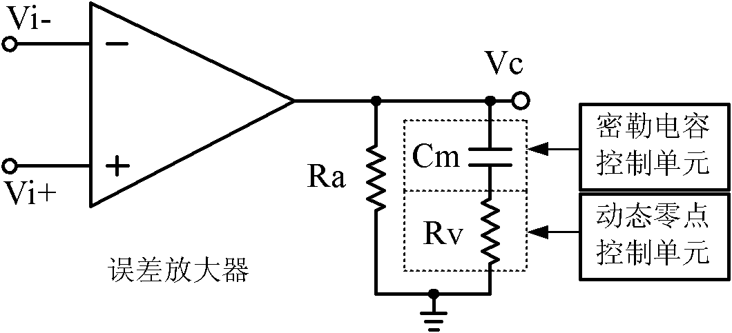
[0054] image 3 The circuit of the frequency compensation network improved by the present invention includes an error amplifier and a frequency compensation circuit.
[0055] Figure 4 The circuit diagram of the error amplifier is given, which adopts a folded cascode structure and consists of a differential input circuit, a common gate amplifier circuit and a current mirror load. The error amplifier includes: a differential input circuit: including a first differential input PMOS transistor M1, a second differential input PMOS transistor M2, and a current mirror PMOS transistor M11; a common-gate amplifier circuit: including a first common-gate NMOS amplifier tube M3, a second common-gate Grid NMOS amplifier tube M4, third common grid NMOS amplifier tube M5 and fourth common grid NMOS amplifier tube M6; a cascode current mirror load: including the first current mirror PMOS load tube M7, the second current mirror PMOS load tube M8 , the third current mirror PMOS load transist...
PUM
 Abstract
Description
Claims
Application Information