Display panel
A technology of display panel and display area, applied in static indicators, nonlinear optics, instruments, etc., to improve anti-peeping effect and reduce side-view brightness
- Summary
- Abstract
- Description
- Claims
- Application Information
AI Technical Summary
Problems solved by technology
Method used
Image

Examples
no. 1 approach
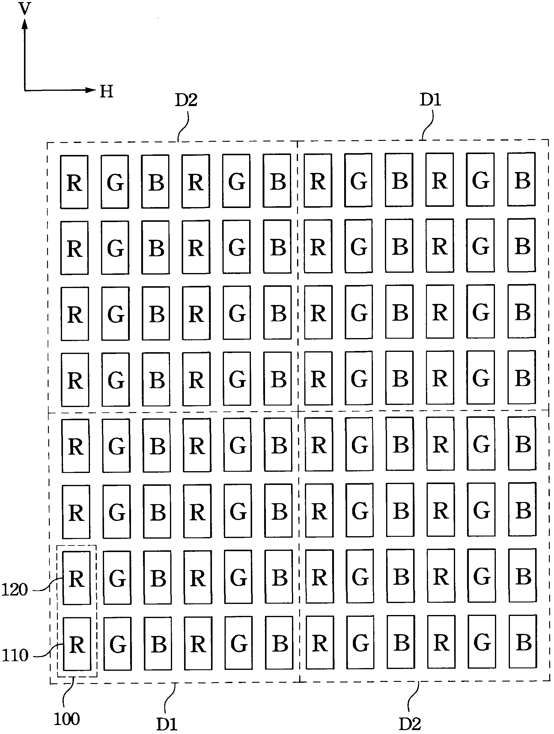
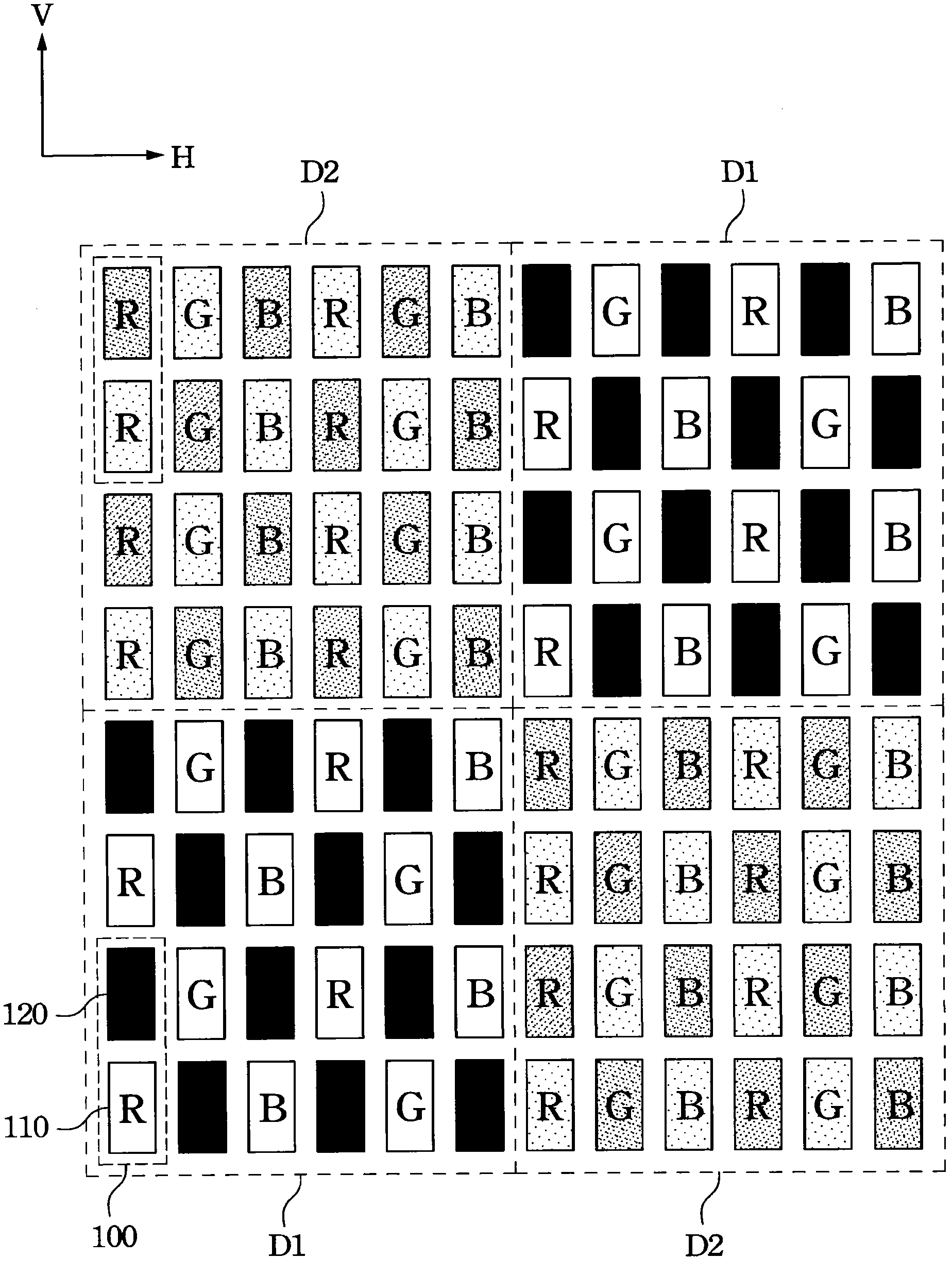
[0099] figure 1 A schematic diagram showing a display panel in a wide viewing angle display mode according to the first embodiment of the present invention. figure 2 show figure 1 The schematic diagram of the display panel in the narrow viewing angle display mode. Such as figure 1 As shown, the display panel of this embodiment includes a first display area D1 (that is, figure 1 upper right display area and lower left display area) and the second display area D2 (that is, figure 1 upper left display area and lower right display area). The first display area D1 and the second display area D2 respectively have a plurality of pixels 100 . Each pixel 100 includes a first sub-pixel 110 and a second sub-pixel 120 . The second sub-pixel 120 is adjacent to the first sub-pixel 110 . Of course, in practical applications, the layout (layout) of the first display area D1 and the second display area D2 of the display panel is not figure 2 and figure 2 As shown only.
[0100] ...
no. 2 approach
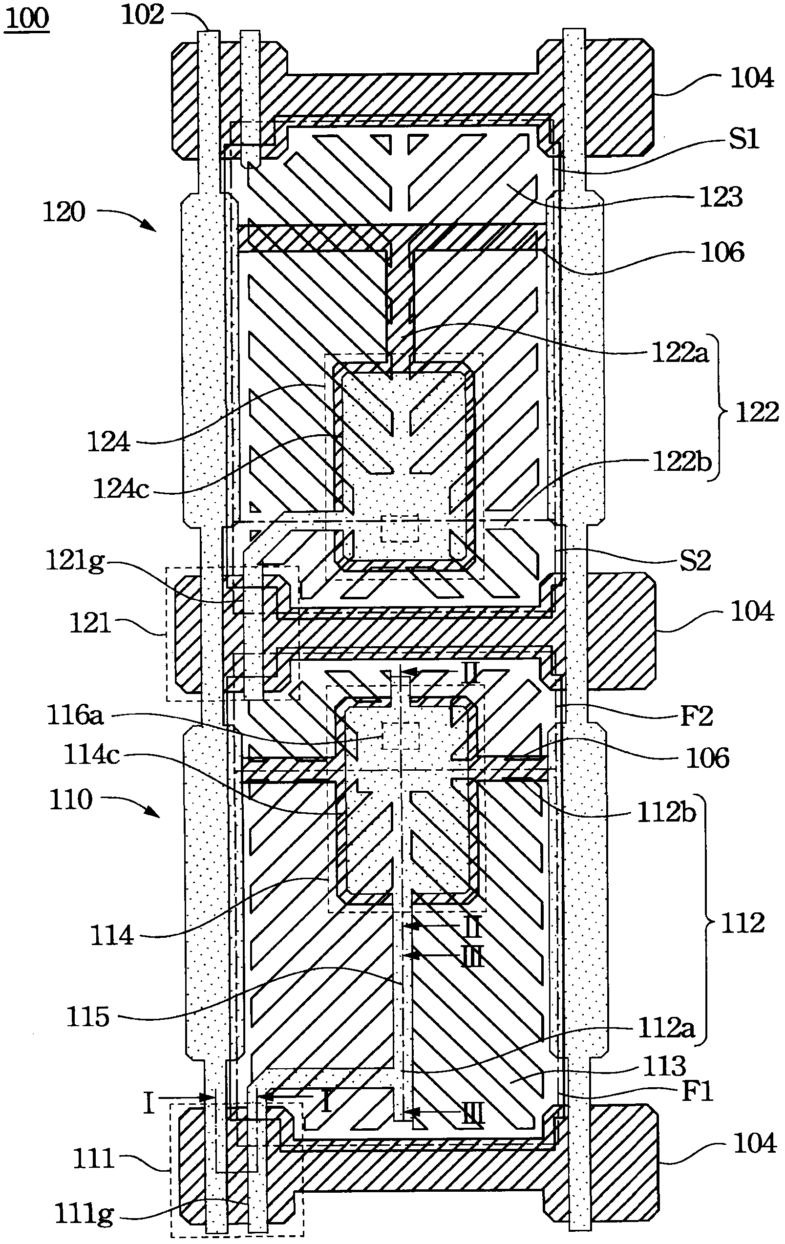
[0122] Figure 5 A top view of a pixel 100 according to a second embodiment of the present invention is shown. The difference between this embodiment and the first embodiment is that in this embodiment, only the first branch pixel electrodes 113 of the first sub-pixel 110 are designed to be misaligned.
[0123] As for other related structures, driving methods and operation details, they are the same as those of the first embodiment, so they will not be repeated here.
no. 3 approach
[0125] Figure 6 A top view of a pixel 100 according to a third embodiment of the present invention is shown. The difference between this embodiment and the first embodiment is that in this embodiment, the first branch pixel electrodes 113 of the first sub-pixel 110 are symmetrically arranged on both sides of the first trunk pixel electrode 112 . That is to say, the first branch pixel electrodes 113 in this embodiment are not designed to be misplaced, but only the first opaque connection lines 115 are at least partially overlapped under the first trunk pixel electrodes 112 .
[0126] As for other related structures, driving methods and operation details, they are the same as those of the first embodiment, so they will not be repeated here.
PUM
 Abstract
Description
Claims
Application Information
 - R&D
- Intellectual Property
- Life Sciences
- Materials
- Tech Scout
- Unparalleled Data Quality
- Higher Quality Content
- 60% Fewer Hallucinations
Browse by: Latest US Patents, China's latest patents, Technical Efficacy Thesaurus, Application Domain, Technology Topic, Popular Technical Reports.
© 2025 PatSnap. All rights reserved.Legal|Privacy policy|Modern Slavery Act Transparency Statement|Sitemap|About US| Contact US: help@patsnap.com