Semiconductor device and manufacturing method thereof

A semiconductor and device technology, applied in the field of semiconductor devices and their manufacturing, can solve problems such as high-concentration doping and large external resistance

Active Publication Date: 2012-08-29
INST OF MICROELECTRONICS CHINESE ACAD OF SCI
View PDF4 Cites 6 Cited by
  • Summary
  • Abstract
  • Description
  • Claims
  • Application Information

AI Technical Summary

Problems solved by technology

In the manufacture of graphene MOS devices, because the graphene layer is too thin, it is difficult to do high concentration doping, so that the external resistance of MOS devices containing graphene is relatively large.

Method used


Image

  • Semiconductor device and manufacturing method thereof
  • Semiconductor device and manufacturing method thereof
  • Semiconductor device and manufacturing method thereof

Examples


Embodiment Construction

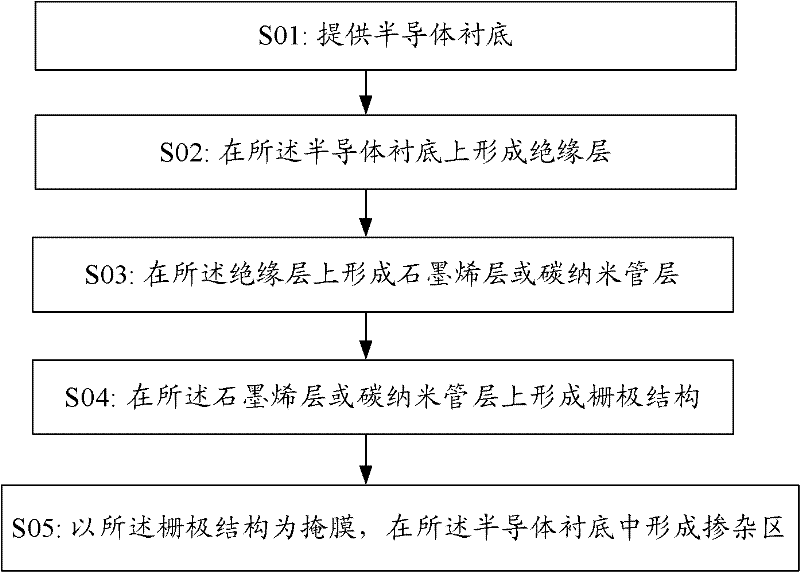
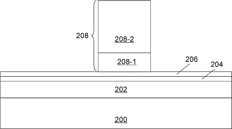
[0010] The following disclosure provides many different embodiments or examples for implementing different structures of the present invention. To simplify the disclosure of the present invention, components and arrangements of specific examples are described below. Of course, they are only examples and are not intended to limit the invention. Furthermore, the present invention may repeat reference numerals and / or letters in different instances. This repetition is for the purpose of simplicity and clarity and does not in itself indicate a relationship between the various embodiments and / or arrangements discussed. In addition, various specific process and material examples are provided herein, but one of ordinary skill in the art will recognize the applicability of other processes and / or the use of other materials. Additionally, configurations described below in which a first feature is "on" a second feature may include embodiments where the first and second features are form...


PUM


Abstract

The invention discloses a semiconductor device and a manufacturing method thereof. The method comprises the following steps of providing a semiconductor substrate; forming an oxide layer on the semiconductor substrate; forming a grapheme layer on the oxide layer; forming a grid medium layer on the grapheme layer; forming a grid electrode on the grid medium layer; patterning the grid electrode; and forming a doping area in the substrate at two sides of the grid electrode. As the doping area is formed in the semiconductor substrate, and then a sensitive doping area is formed on the surface layer of the grapheme layer due to static induction, so as to form doping in the grapheme layer, thus, the decrease of the external resistance of the semiconductor device containing the grapheme layer can be facilitated.

Description

technical field [0001] The present invention generally relates to the technical field of semiconductor manufacturing, and specifically relates to a semiconductor device and a manufacturing method thereof. Background technique [0002] Since its discovery, graphene has become a research hotspot of research groups all over the world. It is a new form of carbon. Due to its unique electrical and physical properties, it has become an ideal material for building nanoelectronic devices. However, in the manufacture of graphene MOS devices, since the graphene layer is too thin, it is difficult to do high-concentration doping, so that the external resistance of the MOS device containing graphene is relatively large. [0003] Therefore, how to form doping in graphene to reduce the external resistance of MOS devices containing graphene has become a technical problem to be solved urgently by those skilled in the art. Contents of the invention [0004] The invention provides a semicond...

Claims


Application Information

Patent Timeline
IPC IPC(8): H01L29/78H01L21/04
Inventor 朱慧珑尹海洲骆志炯
Owner INST OF MICROELECTRONICS CHINESE ACAD OF SCI
Why Eureka
Try Eureka