Array substrate and display device

An array substrate and thin film transistor technology, which is applied in the field of liquid crystal display, can solve the problems of screen flicker and rise, and achieve the effect of stable screen display.

Active Publication Date: 2015-05-13
BOE TECH GRP CO LTD +1
View PDF5 Cites 0 Cited by
  • Summary
  • Abstract
  • Description
  • Claims
  • Application Information

AI Technical Summary

Problems solved by technology

[0003] The array substrate in the prior art has a single-gate structure. Due to the overlap between the drain and the gate in the thin-film transistor, the thin-film transistor has a parasitic capacitance Cgd
like figure 1 As shown, when the switching voltage signal from the gate line controls the thin film transistor to turn on, the data voltage signal from the data line starts to charge the pixel electrode, and the pixel charging voltage on the pixel electrode gradually rises to the set value; when the thin film transistor is turned off At the moment when the switching voltage signal drops to a low level, the charge stored on the parasitic capacitor Cgd will change, which will cause the voltage on the pixel electrode to change, and then cause the voltage on the pixel electrode to generate a jump voltage ΔVp, causing the screen to flicker

Method used


Image

  • Array substrate and display device
  • Array substrate and display device
  • Array substrate and display device

Examples


Embodiment Construction

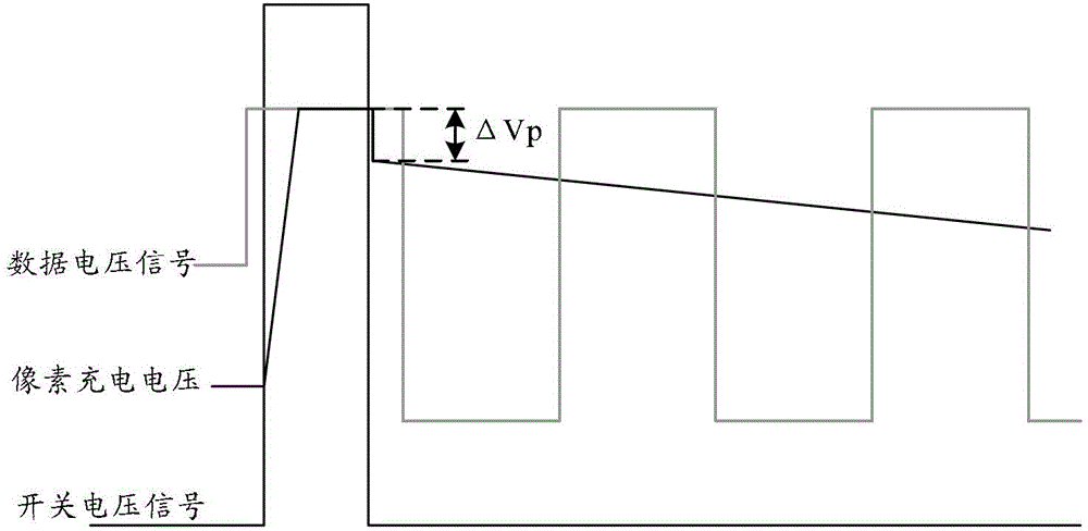
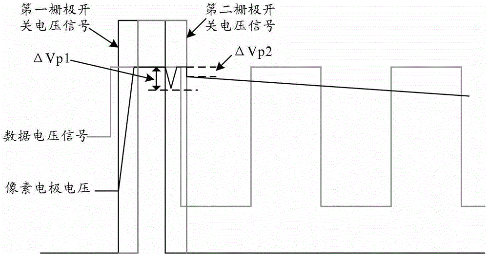
[0020] Embodiments of the present invention provide an array substrate and a liquid crystal display device, which can reduce the jump voltage of the pixel electrode, thereby making the image display more stable.

[0021] In the following description, for purposes of illustration rather than limitation, specific details such as specific system architectures, interfaces, and techniques are set forth in order to provide a thorough understanding of the present invention. It will be apparent, however, to one skilled in the art that the invention may be practiced in other embodiments without these specific details. In other instances, detailed descriptions of well-known devices, circuits, and methods are omitted so as not to obscure the description of the present invention with unnecessary detail.

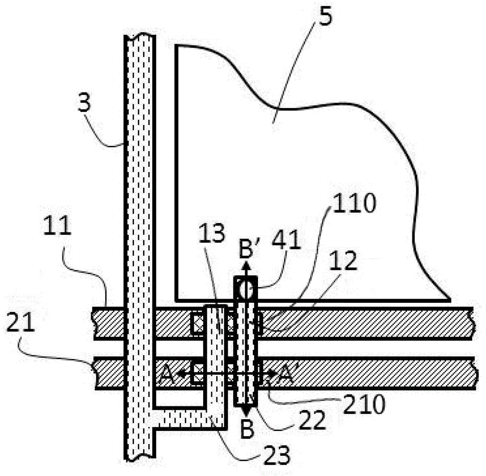
[0022] This embodiment provides an array substrate, such as figure 2 As shown, it includes a pixel electrode 5 and a data line 3 that provides a data voltage signal for the pixel elect...


PUM


Abstract

Embodiments of the present invention disclose an array substrate and a driving method thereof, and a display device. The array substrate comprises: a pixel electrode; a data line; a first thin film transistor comprising a first gate electrode, a first source electrode and a first drain electrode, and a second thin film transistor comprising a second gate electrode, a second source electrode and a second drain electrode; a first gate line connected with the first gate electrode and a second gate line connected with the second gate electrode, wherein the first source electrode and the second source electrode are electrically connected with the data line, and the first drain electrode and the second drain electrode are electrically connected with the pixel electrode.

Description

technical field [0001] The invention relates to the field of liquid crystal display, in particular to an array substrate and a display device. Background technique [0002] Thin Film Transistor-Liquid Crystal Display (TFT-LCD for short) has the advantages of lightness, thinness, and low energy consumption, and is widely used in modern information equipment such as TVs, computers, mobile phones, and digital cameras. TFT-LCD is mainly composed of an array substrate and a color filter substrate, wherein the array substrate includes gates, data lines, pixel electrodes and thin film transistors. When the gate voltage is high, the thin film transistor is turned on, and the pixel electrode is charged through the data line; when the gate voltage is low, the thin film transistor is turned off, and the storage voltage of the pixel electrode will be maintained until the next time the thin film transistor is turned on again. [0003] The array substrate in the prior art has a single ga...

Claims


Application Information

Patent Timeline
Patent Type & Authority Patents(China)
IPC IPC(8): G02F1/1362G02F1/1368H01L27/12
CPCG09G3/3659G02F1/13624G09G2320/0214H01L27/124
Inventor 王盛
Owner BOE TECH GRP CO LTD
Why Eureka
Try Eureka