OLED device

A device and light-emitting layer technology, which is applied in the field of OLED devices, can solve the problems affecting the purity of luminous color of the device, reduce the luminous efficiency, and affect the life of the device, and achieve the effects of strong carrier transport capacity, improved quantum efficiency, and high quantum efficiency

Inactive Publication Date: 2013-11-27
AVIC BEIJING INST OF AERONAUTICAL MATERIALS
View PDF3 Cites 9 Cited by
  • Summary
  • Abstract
  • Description
  • Claims
  • Application Information

AI Technical Summary

Problems solved by technology

[0003] However, due to the relatively long radiation lifetime of triplet phosphorescence, the triplet excitons can easily migrate to the carrier transport layer and cause the material of the transport layer to emit light, thereby reducing the luminous efficiency and affecting the luminous color purity of the device.
The usual solution is to match multilayer auxiliary layers on both sides of the light emitting layer, including hole injection layer, hole transport layer, electron injection layer, electron transport layer and electron blocking layer, etc. However, the addition of multilayer auxiliary layers, on the one hand It increases the manufacturing cost of the device, and on the other hand, it is easy to cause the defect of the device, thus affecting the life of the device

Method used


Image

  • OLED device
  • OLED device
  • OLED device

Examples


Embodiment Construction

[0015] The OLED device of the present invention and its preparation method are described in detail below in conjunction with the accompanying drawings:

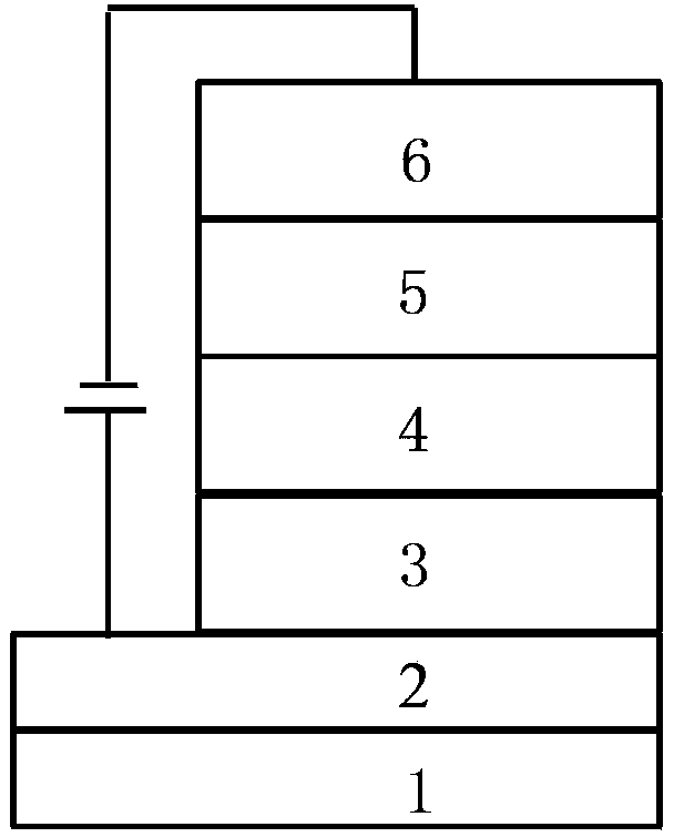
[0016] see figure 1 As shown, the OLED device of the present invention includes a substrate 1, a transparent anode 2, a hole injection layer 3, a light emitting layer 4, an electron injection layer 5 and a cathode 6, the transparent anode 2 is arranged on the substrate 1, and the hole injection layer 3 is arranged On the transparent anode 2 , the light emitting layer 4 is arranged on the hole injection layer 3 , the electron injection layer 5 is arranged on the light emitting layer 4 , and the cathode 6 is arranged on the electron injection layer 5 .

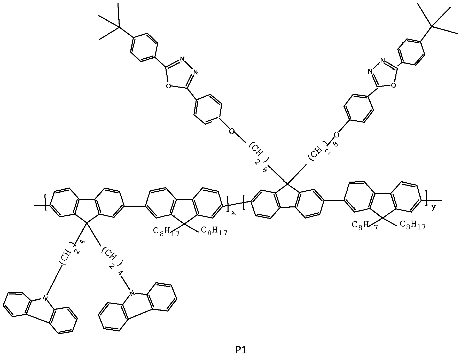
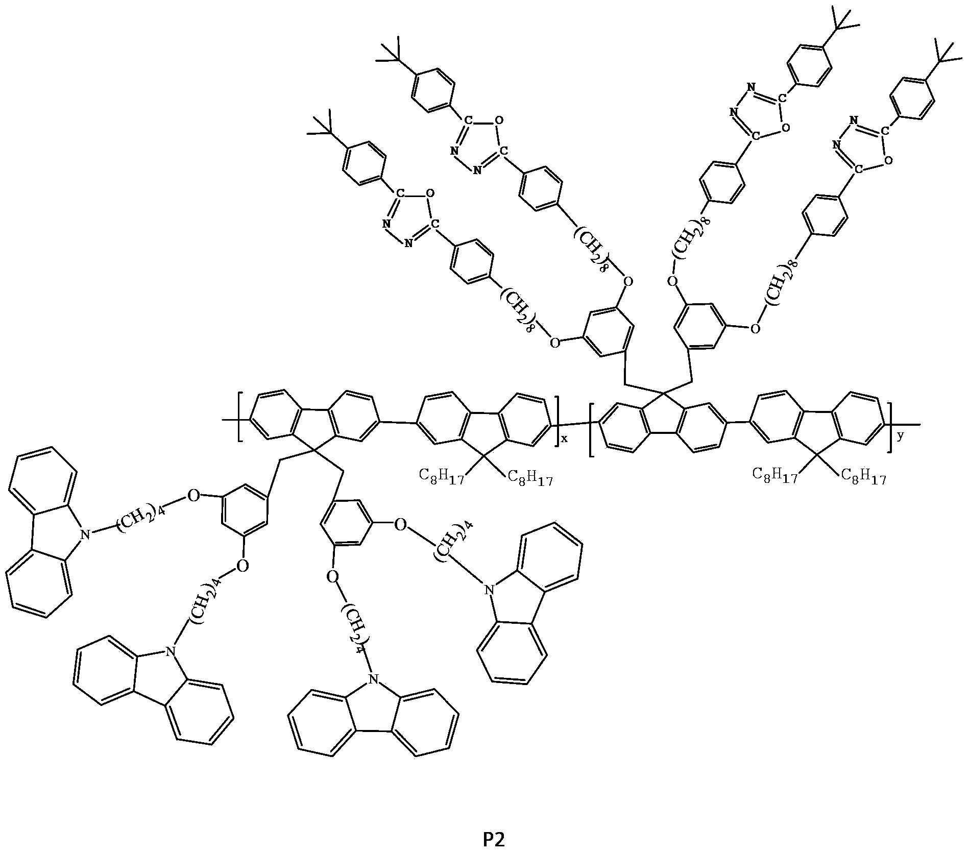
[0017] The substrate 1 of the OLED device is glass, the transparent electrode 2 is an anode ITO film of 20 Ω / □, the hole injection layer 3 is PEDOT:PSS, the light-emitting layer 4 is the doping material listed in Table 1, and the electron injection layer 5 is LiF , the cathode...


PUM

PropertyMeasurementUnit
thicknessaaaaaaaaaa

Abstract

The invention provides an OLED device. The OLED device structurally comprises a substrate (1), a transparent anode (2), a hole injection layer (3), a luminescent layer (4), an electron injection layer (5) and a cathode (6), wherein the luminescent layer (4) is formed by host fluorescent materials and object phosphor materials in a doping mode, and polyfluorene materials which have both hole transport groups and electro-transport groups are adopted by the host fluorescent materials. The OLED device can effectively reduce barriers of hole injection and electron injection and has high quantum efficiency and carrier transport capability.

Description

technical field [0001] The invention is an OLED device and belongs to the technical field of preparation of electronic devices. Background technique [0002] Because OLED has many advantages such as self-illumination, full solid state, wide viewing angle, and fast response, it is considered to have great application prospects in flat panel displays, and is even considered to be a new generation of flat panel displays after liquid crystal (LCD) and plasma (PDP). products and technologies. In order to improve the efficiency of the device, the light-emitting layer usually adopts a host / guest doping system. According to spin statistics, the probability ratio of holes and electrons combining to form singlet and triplet excitons is 1:3, that is, 25% of the excited molecules will form a singlet state, while 75% of the excited molecules will form a triplet state. Due to the restriction of the selection rule, the transition from the triplet state to the ground state of the fluoresc...

Claims


Application Information

Patent Timeline
Patent Type & Authority Applications(China)
IPC IPC(8): H01L51/50H01L51/54C09K11/06C08G61/02
Inventor 宋洪松杨程
Owner AVIC BEIJING INST OF AERONAUTICAL MATERIALS
Why Eureka
Try Eureka