Single photon counting detector system having improved counter architecture

A detector system and single photon counting technology, applied in radiation measurement, TV system components, instruments, etc., can solve problems such as limited statistical data

Active Publication Date: 2013-12-04
PAUL SCHERRER INSTITUT
View PDF4 Cites 31 Cited by
  • Summary
  • Abstract
  • Description
  • Claims
  • Application Information

AI Technical Summary

Problems solved by technology

Since statistics are usually very limited for both pumped and probed measurements, the pump repetition rate needs to be maximized, which prevents reads for every interval (both pumped and non-pumped)
Also for rapidly changing systems it is not always possible to read the detector for every detection interval

Method used


Image

  • Single photon counting detector system having improved counter architecture
  • Single photon counting detector system having improved counter architecture
  • Single photon counting detector system having improved counter architecture

Examples


Embodiment Construction

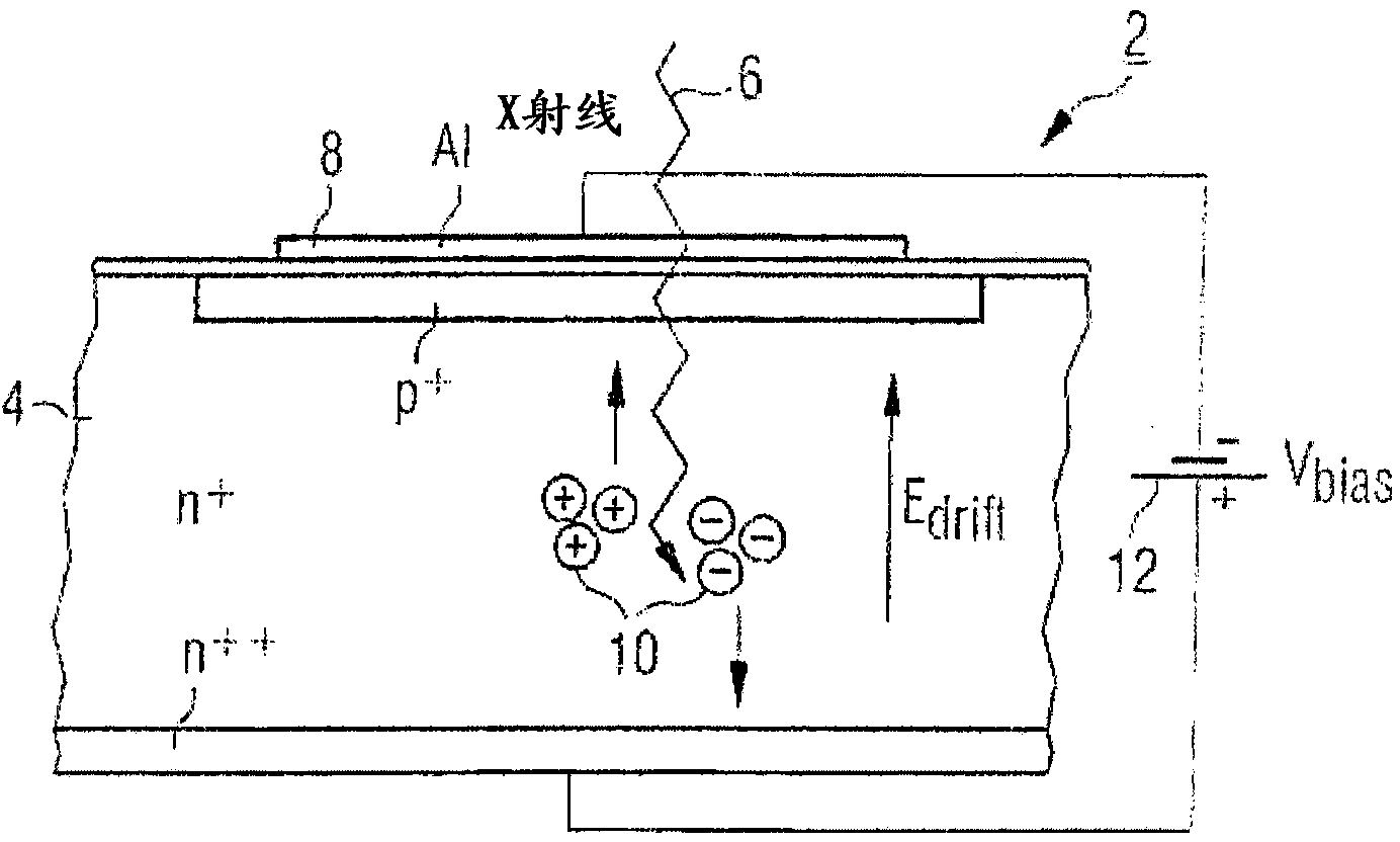
[0029] figure 1 Schematically shows a doped semiconductor p + , n - , n ++ The structure of the photodetector diode 2 of the intrusion part 4 . The most commonly used material is silicon crystal, but germanium, gallium arsenide or cadmium telluride can also be used.

[0030] Incident photons 6 having energies in the range of 100 eV to several Kev are entering the doped semiconductor p + , n - , n ++ The intrusion part 4 is preceded by a possible covering layer (eg aluminum) 8 and after x-ray absorption a corresponding number of electron-hole pairs 10 are generated according to their energy and the energy required to establish them. In the figure, these numbers of electron-hole pairs are exemplarily shown as three electron-hole pairs 10 divided by the electric field generated by the bias voltage source 12 .

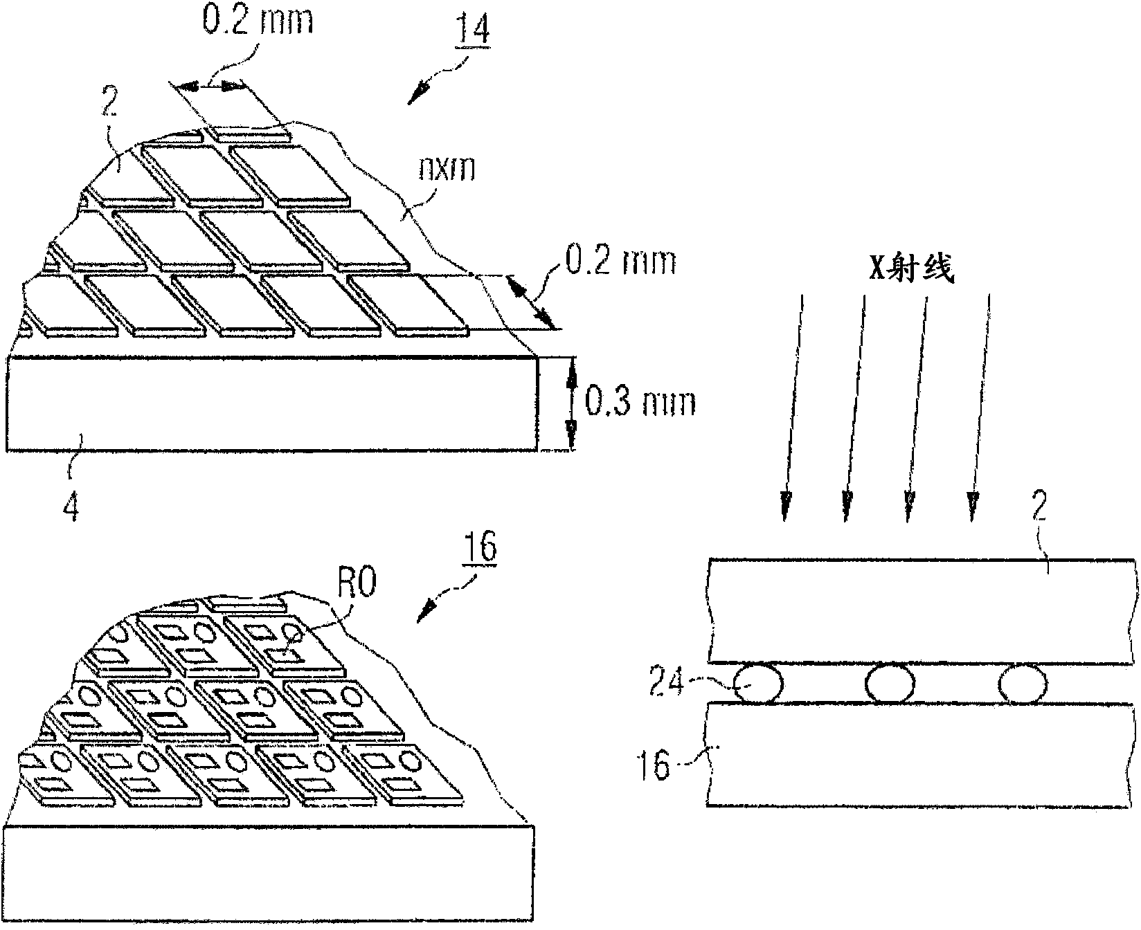
[0031] figure 2A schematic diagram of a two-dimensional pixel detector 14 with a large number of photodetector diodes 2 arranged in an array of n rows and m colum...


PUM


Abstract

The present invention relates to a single photon counting detector system (14), comprising: a) a layer of photosensitive material (4); b) an N×M array of photo-detector diodes (2) arranged in said layer of photosensitive material (4); each of said photo-detector diodes (2) having a bias potential interface (12) and a diode output interface, said bias potential interface (12) of each photo-detector diode (2) being connected to a bias potential (V bias ) ; c) an N×M array of high gain, low noise readout unit cells (RO), one readout unit cell (RO) for each photo-detector diode (2); d) each readout unit cell (RO) comprising: d1) an input interface (IN) connected to said diode output interface, a high-gain voltage amplifying means (amp) comprising an integration capacitor (Cint), d2) at least two parallel lines of digital counters, d3) each line comprising a comparator having an individually selectable threshold (threshold1, threshold2) and a gateable section (gate1, gate2) to determine the counting intervals of the digital counters. e) a multiplexing means allowing to access the readout cell unit either on a per pixel basis or for several pixels in parallel to read out the digital counter to a data processing means transfering the data off the chip to the data processing means, in particular external readout electronics which do not form an integral part of the readout unit cells

Description

technical field [0001] The present invention relates to a single photon counting detector system with an improved counter structure. Background technique [0002] This topic describes readout chips and parts of detector systems in materials science, crystallography, non-destructive testing, and medical applications in synchrotron or x-ray applications using laboratory equipment (laboratory diffractometers). The energy of the photons to be detected is roughly in the range of about 0.1 to 150 keV. [0003] The detector is a hybrid detector comprising an x-ray sensitive layer (silicon sensor) and a readout chip. In the case of a 2-dimensional detector (pixel detector), each pixel in the sensor is directly connected (bump bonded or flip chip bonded) to a corresponding pixel in the readout chip. The size of the pixels is thus limited by the size of the pixels in the readout chip, and due to finding the right balance (pay-off) between the pixel size in the readout chip and the c...

Claims


Application Information

Patent Timeline
Patent Type & Authority Applications(China)
IPC IPC(8): H04N5/3745H04N5/32G01N23/00G01T1/00G01T1/24
CPCH04N5/32H04N5/37455G01T1/247H04N25/772G01T1/29
Inventor 贝恩德·施米特安娜·贝尔加马斯基阿尔多·莫扎尼卡罗伯托·迪纳波利
Owner PAUL SCHERRER INSTITUT
Why Eureka
Try Eureka