Electronic device and manufacturing method thereof

A technology for electronic devices and manufacturing methods, which is applied in the manufacture of semiconductor/solid-state devices, electric solid-state devices, and components of semiconductor/solid-state devices, etc. The effect of saving electromagnetic interference shielding packaging costs, occupying less space on the substrate, and saving packaging costs

Active Publication Date: 2014-01-01
HUAWEI DEVICE CO LTD
View PDF3 Cites 9 Cited by
  • Summary
  • Abstract
  • Description
  • Claims
  • Application Information

AI Technical Summary

Problems solved by technology

However, the metal shielding frame 101 increases the overall height of the plastic package module, and the plastic sealant can only penetrate into the metal shield frame 101 through the through hole 102 on the metal shield frame 101, and the fluidity of the plastic sealant is poor.
Therefore, the effect of shielding electronic components through metal shielding frames is not good

Method used


Image

  • Electronic device and manufacturing method thereof
  • Electronic device and manufacturing method thereof
  • Electronic device and manufacturing method thereof

Examples


Embodiment Construction

[0037] In order to make the purpose, technical solutions and advantages of the present invention clearer, the technical solutions in the present invention will be clearly and completely described below in conjunction with the accompanying drawings of the present invention. Obviously, the described embodiments are part of the embodiments of the present invention. rather than all examples. Based on the embodiments of the present invention, all other embodiments obtained by persons of ordinary skill in the art without creative efforts fall within the protection scope of the present invention.

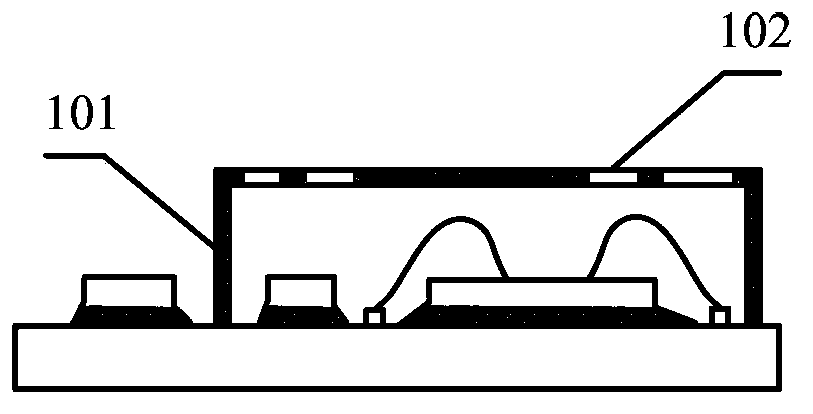
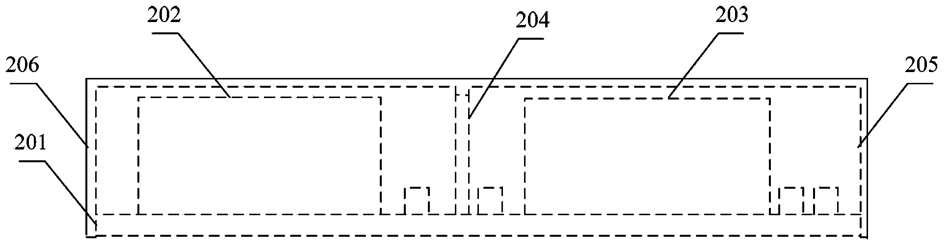
[0038] figure 2 The schematic diagram of the cross-sectional structure of the electronic device provided by the embodiment of the present invention, such as figure 2 As shown, the electronic device includes a substrate 201 , a first electronic component 202 , a second electronic component 203 , a metal shielding wall 204 , a plastic sealant 205 and a conductive film 206 .

[0039] A gr...


PUM


Abstract

The embodiment of the invention provides an electronic device and a manufacturing method thereof. The electronic device comprises a substrate, which is provided with a grounding layer; a first electronic element and a second electronic element, which are disposed on the substrate; a metal shielding wall, which is disposed between the first electronic element and the second element; a plastic sealing rubber, which can be used to wrap the first electronic element, the second electronic element, and the metal shielding wall, and is provided with an opening; a conductive film, which is used to wrap a metal surface exposed from the opening of the metal surface of the top of the metal shielding wall, and is electrically connected with the grounding layer of the substrate. The electronic device and the manufacturing method thereof have advantages of better electromagnetic interference shielding effect, and ability of saving electromagnetic interference shielding packaging costs of electronic elements.

Description

technical field [0001] Embodiments of the present invention relate to electromagnetic interference shielding technologies, and in particular to an electronic device and a method for manufacturing the electronic device. Background technique [0002] The electromagnetic interference shielding design can reduce the external radiation interference of electronic components, and can also reduce the interference of external radiation on electronic components. Many electronic components require electromagnetic interference shielding design. For example, in IC design, it is necessary to separate the radio frequency electronic components from the surrounding electronic components. [0003] In the prior art, a commonly used shielding method for electronic components is mainly to realize the shielding of electronic components through a metal shielding frame. [0004] figure 1 It is a schematic structural diagram of a metal shielding frame in the prior art, such as figure 1 As shown, ...

Claims


Application Information

Patent Timeline
Patent Type & Authority Applications(China)
IPC IPC(8): H01L23/552H01L23/31H01L21/56
CPCH01L2224/48091H01L23/3121H01L2224/73265H01L23/552H01L2224/48227H01L2224/32225H01L2924/3025H01L2924/19105H01L2924/00014H01L2924/00
Inventor 杨宇占奇志
Owner HUAWEI DEVICE CO LTD
Why Eureka
Try Eureka