Check patentability & draft patents in minutes with Patsnap Eureka AI!

Method for detecting edge defect of wafer

A technology of edge defects and detection methods, applied in semiconductor/solid-state device testing/measurement, electrical components, circuits, etc., can solve the problem that the coordinate map cannot correctly display wafer edge defects, etc.

Active Publication Date: 2015-01-14
SEMICON MFG INT (SHANGHAI) CORP
View PDF3 Cites 5 Cited by
  • Summary
  • Abstract
  • Description
  • Claims
  • Application Information

AI Technical Summary

Problems solved by technology

[0006] The purpose of the present invention is to provide a method for detecting wafer edge defects to solve the problem that existing two-dimensional defect coordinate maps cannot correctly display wafer edge defects

Method used


Image

  • Method for detecting edge defect of wafer
  • Method for detecting edge defect of wafer
  • Method for detecting edge defect of wafer

Examples


Embodiment Construction

[0028] The method for detecting wafer edge defects proposed by the present invention will be further described in detail below with reference to the accompanying drawings and specific embodiments. Advantages and features of the present invention will be apparent from the following description and claims. It should be noted that all the drawings are in a very simplified form and use imprecise scales, and are only used to facilitate and clearly assist the purpose of illustrating the embodiments of the present invention.

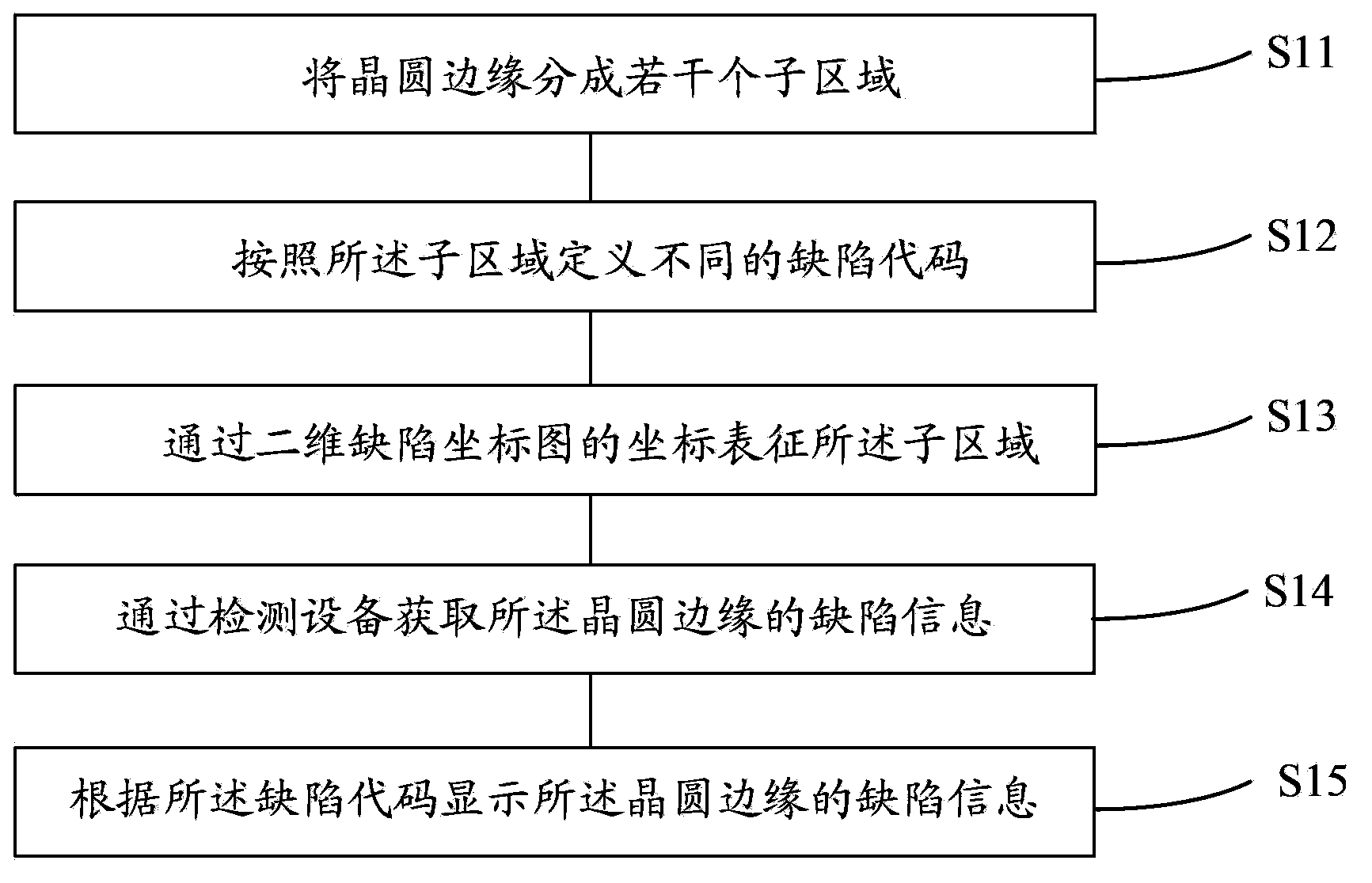
[0029] Please refer to image 3 , which is a flowchart of a method for detecting wafer edge defects according to an embodiment of the present invention. Such as image 3 Shown, the detection method of described wafer edge defect comprises the following steps:

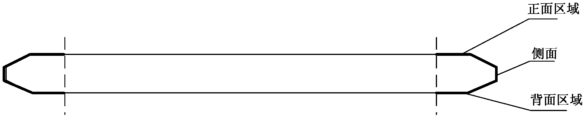
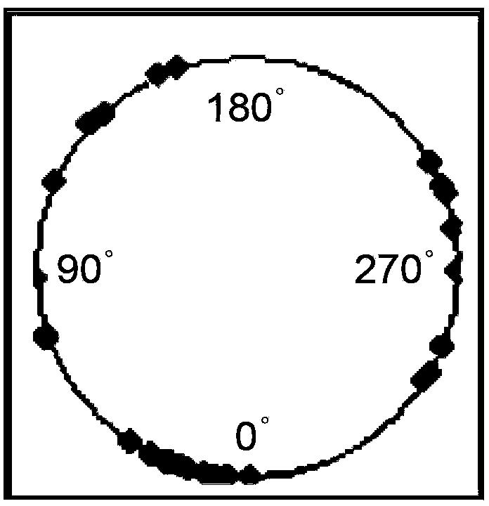
[0030] S11: dividing the edge of the wafer into several sub-regions;

[0031] S12: Define different defect codes according to the sub-areas;

[0032] S13: Characterize the sub-region by the coordina...


PUM


Abstract

The invention provides a method for detecting an edge defect of a wafer. The method for detecting the edge defect of the wafer comprises the steps that the edge of the wafer is divided into multiple sub-areas, different defect codes are defined according to the sub-areas, the sub-areas are represented through coordinates of a two-dimensional defect coordinate graph, edge defect information of the wafer is obtained through a detection device, and the edge defect information of the wafer is displayed according to the defect codes. According to the method for detecting the edge defect of the wafer, the positions where edge defects are located are distinguished according to the different defect codes, and thus the edge defect of the wafer can be displayed correctly through the two-dimensional defect coordinate graph.

Description

technical field [0001] The invention relates to the technical field of integrated circuit manufacturing, in particular to a method for detecting wafer edge defects. Background technique [0002] For many years, the wafer surface, both the front side of the wafer and the back side of the wafer, has been the focus of defect inspection. The edge of the wafer is considered less important and is generally not inspected for defects. However, during the manufacturing process, it was found that the edge of the wafer is very prone to scratches or residual foreign matter. These defects will become a source of pollution, diffuse to the inner area and surface of the wafer, and affect the devices inside the wafer. As the feature size continues to shrink, devices are getting closer and closer to the edge of the wafer, and the impact of wafer edge defects on the process and product yield is increasing, especially in the manufacturing process of 65nm and below, wafer edge defects The tech...

Claims


Application Information

Patent Timeline
IPC IPC(8): H01L21/66
CPCH01L22/12
Inventor 翟云云戴腾
Owner SEMICON MFG INT (SHANGHAI) CORP
Features
  • R&D
  • Intellectual Property
  • Life Sciences
  • Materials
  • Tech Scout
  • Unparalleled Data Quality
  • Higher Quality Content
  • 60% Fewer Hallucinations
Learn More