

Solid-state imaging device
A solid-state imaging device and pixel technology, which is applied in the direction of electric solid-state devices, radiation control devices, transistors, etc., can solve the problems of signal-to-noise ratio degradation and signal volume reduction, and achieve the effect of suppressing color mixing and improving sensitivity
- Summary
- Abstract
- Description
- Claims
- Application Information
AI Technical Summary
Problems solved by technology
Method used
Image

Examples
no. 1 approach
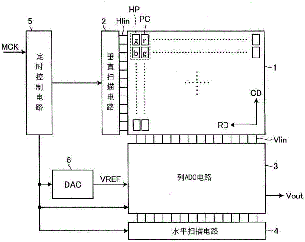
[0038] figure 1 It is a block diagram showing a schematic configuration of the solid-state imaging device according to the first embodiment.
[0039] exist figure 1 Among them, the solid-state imaging device is provided with: a pixel array section 1 in which pixels PC storing photoelectrically converted charges are arranged in a matrix in the row direction and in the column direction; and a vertical scanning circuit 2 in the vertical direction to be read out Column ADC circuit 3 detects the signal components of each pixel PC through CDS; horizontal scanning circuit 4 scans the pixel PC to be read out along the horizontal direction; timing control circuit 5 scans each pixel PC The timing of reading and accumulation of the PC is controlled; and the reference voltage generating circuit 6 outputs the reference voltage VREF to the column ADC circuit 3 . In addition, the master clock MCK is input to the timing control circuit 5 .
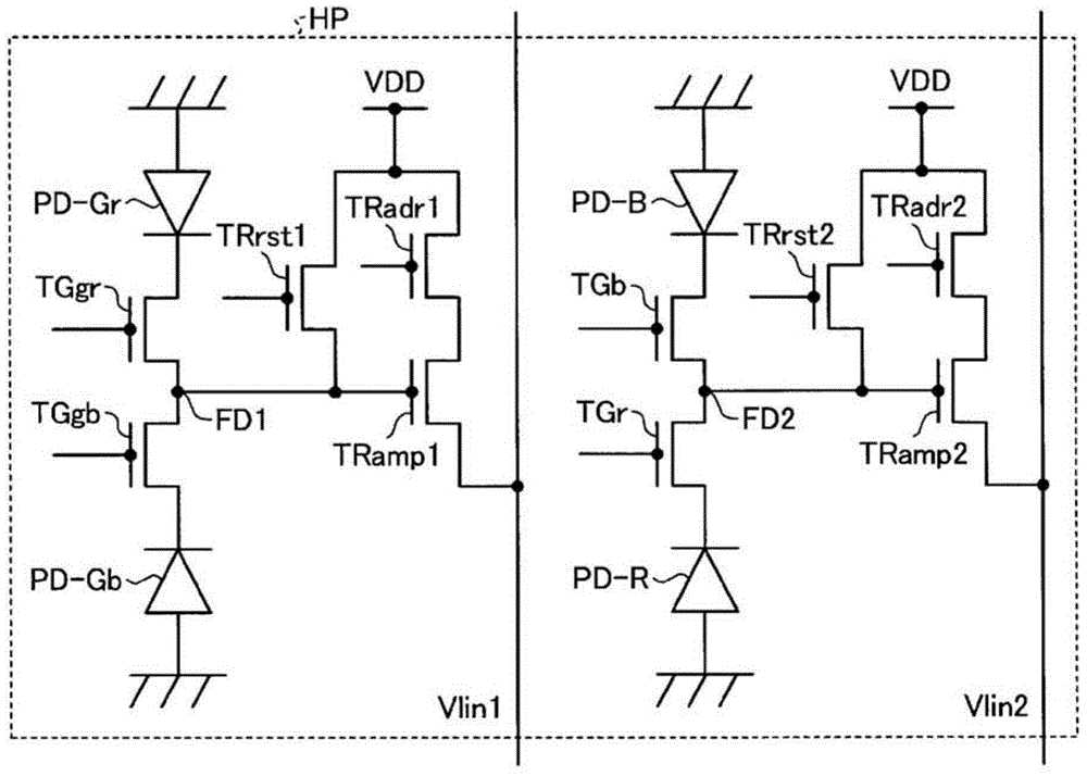
[0040] Here, in the pixel array section 1, a hor...
no. 2 approach
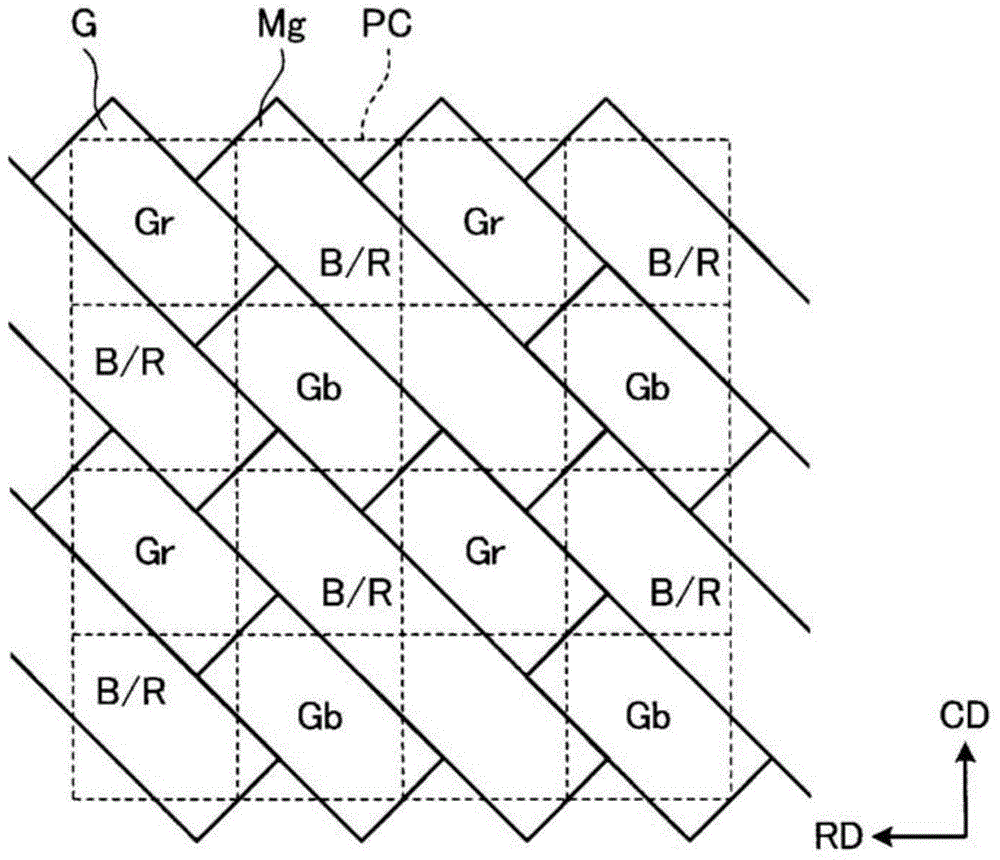
[0071] Figure 10 (a) is a plan view showing an example of the layout of the color filter of the solid-state imaging device according to the second embodiment, Figure 10 (b) is a plan view showing an example of the layout of the microlenses of the solid-state imaging device according to the second embodiment.
[0072] exist Figure 10 In (a), in this solid-state imaging device, the image 3 The composition of the increased light-shielding film SH. In addition, the material of the light shielding film SH may be a resin containing carbon or the like, or a metal such as aluminum or tungsten. Here, the light-shielding film SH can be arranged so as to cover the lead-out portion that leads the pixel B for blue arranged below the pixel R for red to the front side. As a result, in the backside illumination type CMOS sensor, it is possible to suppress red light from entering the blue pixels B, and to reduce color mixing.
[0073] In addition, in Figure 10 In (b), on the magenta...
no. 3 approach
[0077] Figure 12 (a) is a plan view showing an example of the layout of the color filter of the solid-state imaging device according to the third embodiment, Figure 12 (b) is a plan view showing another layout example of the color filter of the solid-state imaging device according to the third embodiment.
[0078] exist Figure 12 In (a), in this solid-state imaging device, instead of image 3 A magenta filter Mg is provided, and a white filter W is arranged on the red pixel R and the blue pixel B. Thereby, the light loss due to the magenta filter Mg can be reduced, and the sensitivity can be increased.
[0079] In addition, in Figure 12 In (b), in this solid-state imaging device, the Figure 12 The structure of (a) adds the light-shielding film SH. Figure 12 The light-shielding film SH of (b) can be combined with Figure 10 The light-shielding film SH of (a) is arranged in the same manner.
[0080] Figure 13 means along Figure 12 (a) A cross-sectional view of ...
PUM
 Abstract
Description
Claims
Application Information