Solid-state imaging apparatus, method for manufacturing the same, and electronic device

a technology of solid-state imaging and manufacturing methods, applied in the direction of radio frequency controlled devices, instruments, television systems, etc., can solve the problems of color separation and s/n deterioration, and achieve the effect of suppressing the occurrence of color mixing between pixels

Active Publication Date: 2019-07-04
SONY SEMICON SOLUTIONS CORP
View PDF8 Cites 5 Cited by
  • Summary
  • Abstract
  • Description
  • Claims
  • Application Information

AI Technical Summary

Benefits of technology

[0012]According to the present technology, occurrence of color mixing between pixels can be suppressed. Note that the effects described here are not necessarily limited, and may be any of the effects described in the present disclosure.

Problems solved by technology

As a result, color mixing occurs between the visible light pixel and the infrared light pixel, and color separation and S / N deteriorate.

Method used


Image

  • Solid-state imaging apparatus, method for manufacturing the same, and electronic device
  • Solid-state imaging apparatus, method for manufacturing the same, and electronic device
  • Solid-state imaging apparatus, method for manufacturing the same, and electronic device

Examples


first embodiment

3. First Embodiment

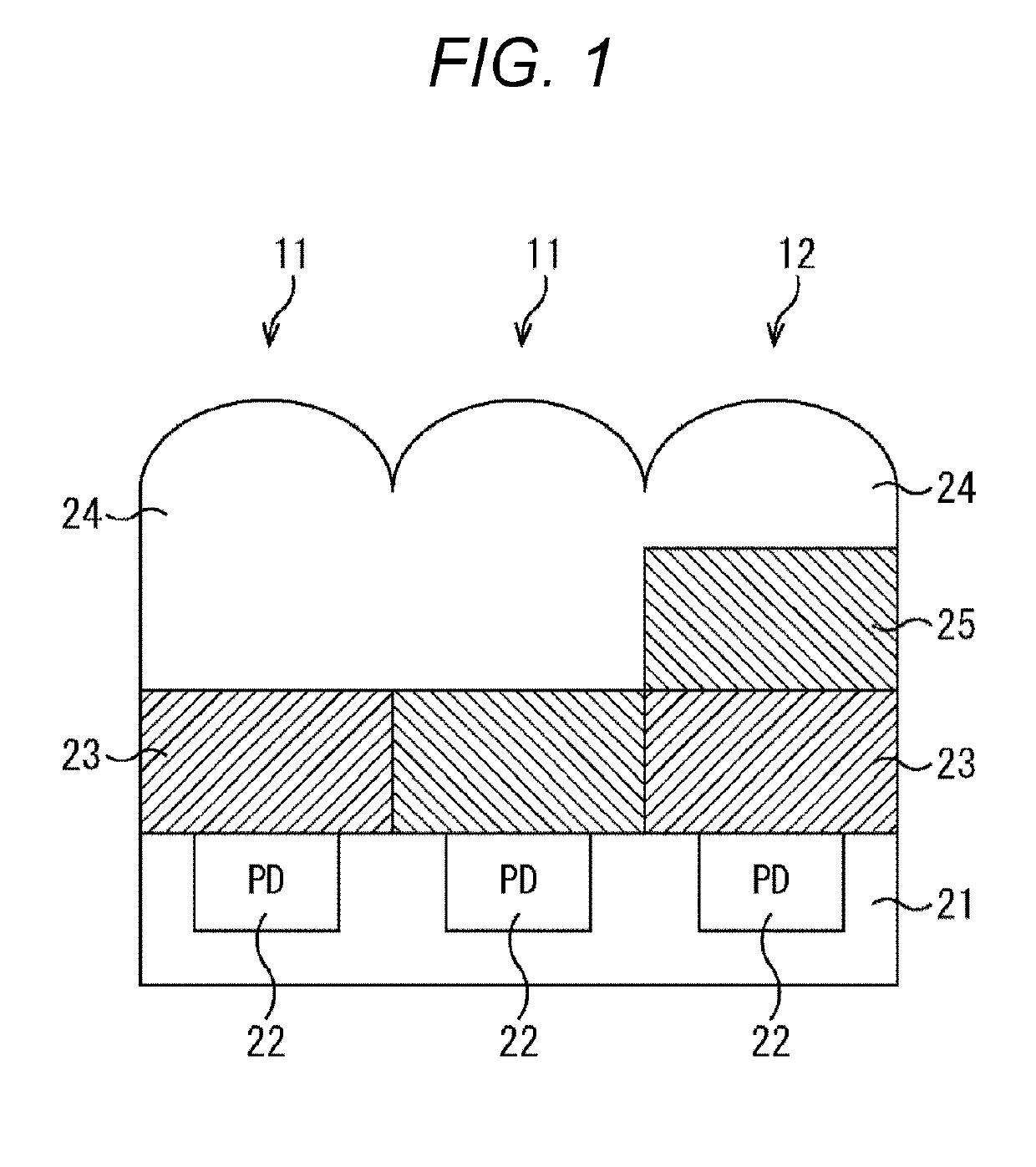
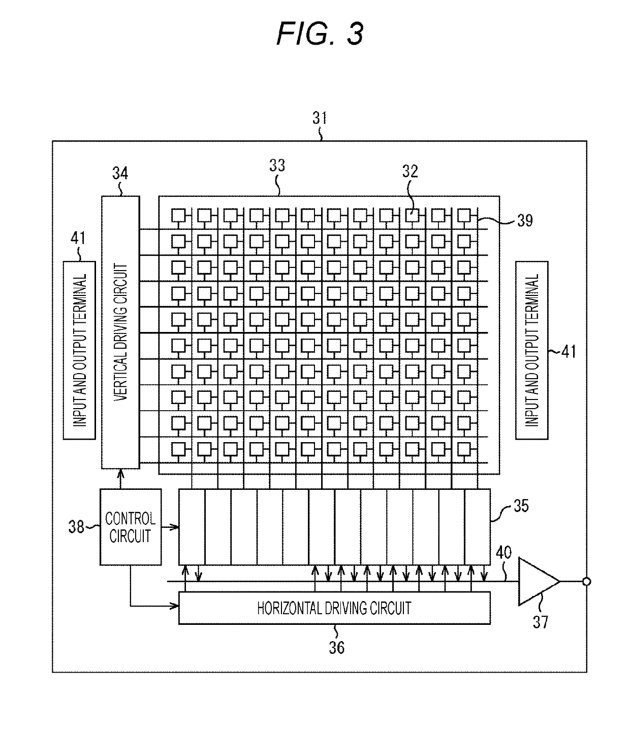
[0111]In a solid-state imaging apparatus 31 according to a first embodiment of the present technology, as a plurality of pixels 32 arranged in a pixel region 33, a visible light pixel and an infrared light pixel are disposed.

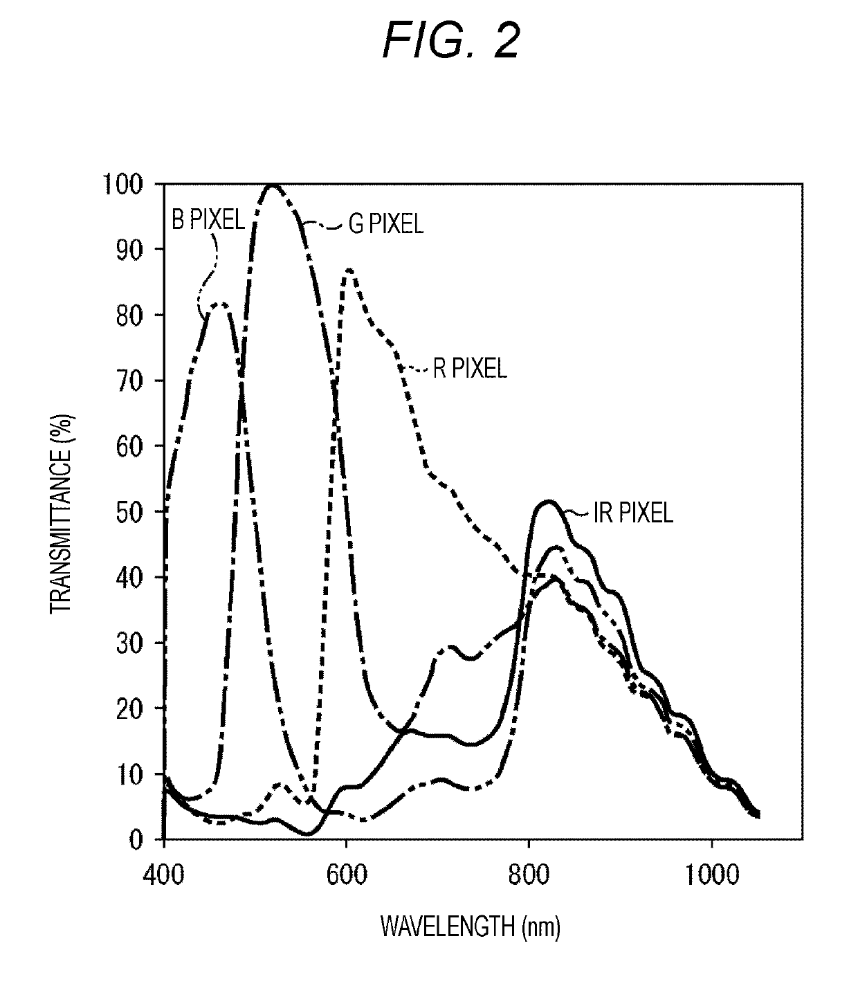
[0112]FIG. 4 is a cross-sectional view illustrating a configuration example of a pixel in the solid-state imaging apparatus 31 according to the first embodiment of the present technology. FIG. 4 illustrates a cross-sectional view of a visible light pixel 51 and an infrared light pixel 52 in the solid-state imaging apparatus 31. The visible light pixel 51 is constituted as, for example, three types of pixels of a red (R) pixel, a green (G) pixel, and a blue (B) pixel.

[0113]In the visible light pixel 51, a photoelectric conversion unit 62 constituted by a photodiode (PD) that receives incident light and performs photoelectric conversion is formed on a semiconductor substrate 61. On the semiconductor substrate 61, an insulating layer (not illustr...

second embodiment

4. Second Embodiment

[0203]In a solid-state imaging apparatus 31 according to a second embodiment of the present technology, only visible light pixels are disposed as a plurality of pixels 32 arranged in a pixel region 33.

[0204]FIG. 35 is a cross-sectional view illustrating a configuration example of a pixel in the solid-state imaging apparatus 31 according to the second embodiment of the present technology. FIG. 35 illustrates a cross-sectional view of a visible light pixel 51 in the solid-state imaging apparatus 31. The visible light pixel 51 is constituted as, for example, three types of pixels of a red (R) pixel, a green (G) pixel, and a blue (B) pixel.

[0205]As in the first embodiment, in the visible light pixel 51, a photoelectric conversion unit 62 constituted by a photodiode (PD) that receives incident light and performs photoelectric conversion is formed on a semiconductor substrate 61. On the semiconductor substrate 61, an insulating layer (not illustrated) including SiO or ...

modification example

[0252]As in the first embodiment, also in the present embodiment, the color filter 66 as the second optical filter layer is formed directly on the first optical filter layer.

[0253]The present invention is not limited thereto. As illustrated in FIG. 49, an organic film 111 may be formed between the first optical filter layer (infrared cut filter 63) and the second optical filter layer (color filter 66). Similarly, as illustrated in FIG. 50, an inorganic film 121 may be formed between the first optical filter layer (infrared cut filter 63) and the second optical filter layer (color filter 66).

[0254]Moreover, as illustrated in FIG. 51, an organic film 151 may be formed between the second optical filter layer (color filter 66) and the microlens 67. Similarly, as illustrated in FIG. 52, an inorganic film 161 may be formed between the second optical filter layer (color filter 66) and the microlens 67.

[0255]Note that it is also possible to combine the structure of FIG. 51 or 52 with each o...


PUM


Abstract

The present technology relates to a solid-state imaging apparatus capable of suppressing occurrence of color mixing, a method for manufacturing the solid-state imaging apparatus, and an electronic device. The solid-state imaging apparatus includes a plurality of pixels arranged in a pixel region. Each of the pixels has: a first optical filter layer disposed on a photoelectric conversion unit; a second optical filter layer disposed on the first optical filter layer; and a separation wall separating at least a part of the first optical filter layer for each of the pixels. Either the first optical filter layer or the second optical filter layer in at least one of the pixels is formed by an infrared cut filter, while the other is formed by a color filter. The present technology can be applied to a CMOS image sensor including a visible light pixel.

Description

TECHNICAL FIELD[0001]The present technology relates to a solid-state imaging apparatus, a method for manufacturing the solid-state imaging apparatus, and an electronic device, and particularly to a solid-state imaging apparatus capable of suppressing occurrence of color mixing, a method for manufacturing the solid-state imaging apparatus, and an electronic device.BACKGROUND ART[0002]Conventionally, a solid-state imaging apparatus that performs imaging using visible light and imaging using infrared light is known.[0003]In such a solid-state imaging apparatus, an infrared light pixel can be formed, for example, by overlapping red (R) and blue (B) color filters. In this case, all the pixels (visible light pixel and infrared light pixel) have substantia the same transmittance in an infrared light region with a wavelength of 700 nm or more. As a result, color mixing occurs between the visible light pixel and the infrared light pixel, and color separation and S / N deteriorate.[0004]Meanwhi...

Claims


Application Information

Patent Timeline
Patent Type & Authority Applications(United States)
IPC IPC(8): H01L27/146G02B5/22H04N5/374
CPCH01L27/14621G02B5/223H01L27/14643H01L27/1463H01L27/14689H01L27/14627H04N5/374H01L27/146G02B5/201G02B5/208H04N23/12H04N25/76
Inventor NAKAJIKI, SINTAROSAYAMA, YUKIHIRO
Owner SONY SEMICON SOLUTIONS CORP
Why Eureka
Try Eureka