Display substrate and preparation method thereof as well as display panel and display device

一种显示基板、显示区的技术,应用在半导体/固态器件制造、仪器、半导体器件等方向,能够解决难以满足显示面板高分辨率的要求、显示面板结构不稳定、易残留黑矩阵材料等问题,达到省去技术难点、减少生产工艺流程、减少工艺流程的效果

Inactive Publication Date: 2015-07-01
HEFEI XINSHENG OPTOELECTRONICS TECH CO LTD +1
View PDF4 Cites 12 Cited by
  • Summary
  • Abstract
  • Description
  • Claims
  • Application Information

AI Technical Summary

Problems solved by technology

[0006] However, in the above-mentioned TFT LCD using the COA technology, it is difficult to form the pattern of the black matrix 12 on the first insulating layer 11. The specific performance is that based on the characteristics of the existing materials for preparing the black matrix 12, it is difficult to meet the display requirements. High resolution requirements of the panel; the material of the black matrix 12 and the material of the first insulating layer 11 (SiN x etc.) insufficient adhesion, which will lead to unstable structure of the display panel; after the development step of the photolithography process for forming the black matrix 12 pattern, the surface of the first insulating layer 11 is likely to remain black matrix material, which will cause cause bad display

Method used


Image

  • Display substrate and preparation method thereof as well as display panel and display device
  • Display substrate and preparation method thereof as well as display panel and display device
  • Display substrate and preparation method thereof as well as display panel and display device

Examples


Embodiment Construction

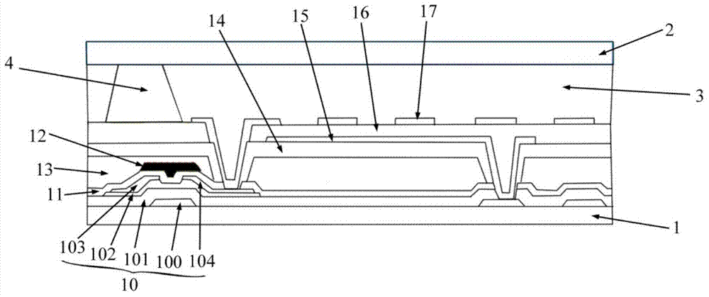
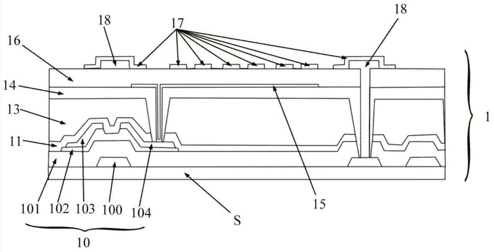
[0049] Specific embodiments of the present invention will be described in detail below in conjunction with the accompanying drawings. It should be understood that the specific embodiments described here are only used to illustrate and explain the present invention, and are not intended to limit the present invention.

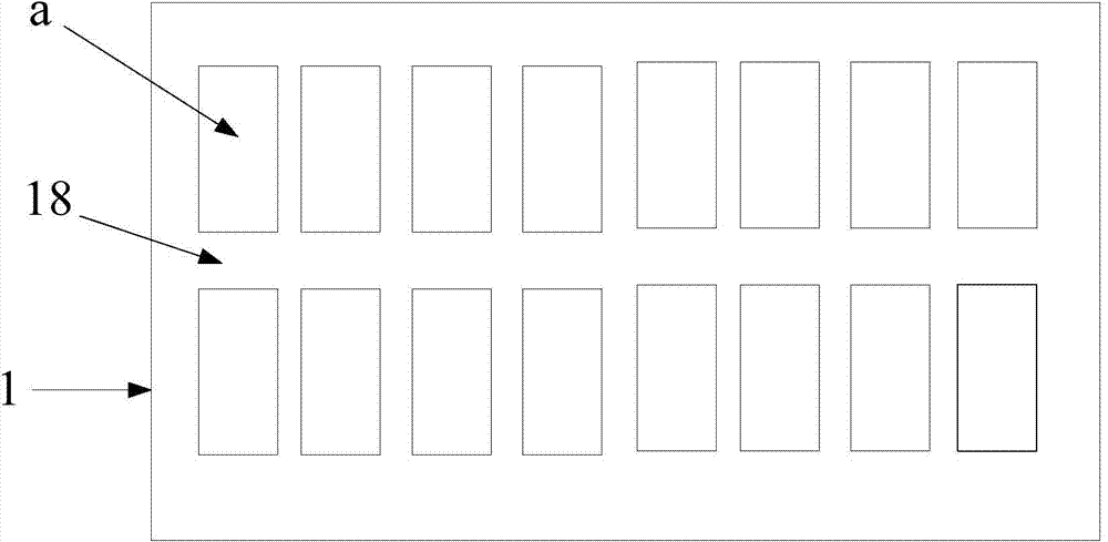
[0050] The present invention provides an embodiment of a display substrate, figure 2 It is a schematic diagram of a display substrate provided by an embodiment of the present invention. Such as figure 2 As shown, in this embodiment, the display substrate 1 includes a plurality of pixels, each pixel has a display area a, and the display area a of the plurality of pixels is a non-display area, and the display substrate 1 also includes a protective Metal layer 18, the protection metal layer 18 covers the non-display area.

[0051] Specifically, the display area a of each pixel is generally the area where the pixel electrode in the pixel is located, and the non...


PUM


Abstract

The invention relates to a display substrate and a preparation method thereof as well as a display panel and a display device. The display substrate comprises a plurality of pixels, wherein each pixel is provided with a display zone; non-display zones are arranged among the display zones of the multiple pixels; the display substrate also comprises protecting metal layers which cover the non-display zones; in the display substrate, the protecting metal layers cover the non-display zones of the display substrate and shield thin film transistors, all signal cables and other structures on the display substrate, and a black matrix can be omitted, so that the flow of a production process can be reduced, the production efficiency is improved, and the production cost is reduced; meanwhile, technical difficulties in the preparation process of the black matrix can be overcome, so that process difficulties in the preparation process of the display substrate are favorably reduced.

Description

technical field [0001] The present invention relates to the field of display technology, in particular, to a display substrate and a preparation method thereof, a display panel and a display device. Background technique [0002] A Thin Film Transistor Liquid Crystal Display (hereinafter referred to as TFT LCD) includes a first substrate and a second substrate that are boxed together, and a liquid crystal layer located between the first substrate and the second substrate. [0003] In an existing TFT LCD, a thin film transistor is prepared on the first substrate, and the thin film transistor is used as a driving switch; a color film and a black matrix are prepared on the second substrate, and the color film is used to realize color display. The black matrix is ​​used to shield the thin film transistors and each signal line. In this kind of TFT LCD, when the first substrate and the second substrate are aligned with the box, there will inevitably be a deviation in the box. Ther...

Claims


Application Information

Patent Timeline
Patent Type & Authority Applications(China)
IPC IPC(8): H01L27/12H01L21/77
CPCG02F1/134363H01L29/78633H01L27/124G02F1/133357G02F1/136222G02F1/13629G02F1/136218G02F1/136295G02F1/13439G02F1/136209G02F1/136286G02F1/1368G02F2201/121G02F2202/16
Inventor 操彬彬江鹏陈鹏文锺源黄寅虎杨成绍杨海鹏
Owner HEFEI XINSHENG OPTOELECTRONICS TECH CO LTD
Why Eureka
Try Eureka